
low frequency sinewave generators

The circuit employs an RC network to create a phase shift necessary for oscillation. The arrangement consists of resistors and capacitors that dictate the frequency of oscillation based on the RC time constant. The phase shift introduced by the RC network is a fundamental aspect of sine wave generation, as it allows the signal to complete a full cycle, resulting in a 360-degree phase shift.
In the transistor circuit, the 3904 NPN transistor functions as an amplifier, where the input signal is applied to the base terminal. The output at the collector terminal is a sine wave, which is then buffered by a Junction Field Effect Transistor (JFET). This buffering stage is critical as it converts the high impedance output of the transistor into a low impedance output, making it suitable for driving loads or interfacing with other circuits without significant signal degradation.
The gain of the circuit is a vital parameter, as it directly impacts the distortion levels of the output signal. An improperly set gain can lead to clipping or other forms of distortion, thereby compromising the quality of the sine wave. The 500-ohm resistor plays a pivotal role in setting this gain; adjustments may be necessary to optimize performance and achieve the desired waveform characteristics.
Despite its theoretical applications, the practical use of this transistor circuit is limited. The requirement for precise adjustments can render the circuit unstable in real-world scenarios, making it less reliable for consistent sine wave generation. Alternative methods or circuits may be preferred for applications demanding higher stability and lower distortion in sine wave outputs.The two circuits illustrate generating low frequency sinewaves by shifting the phase of the signal through an RC network so that oscillation occurs where the total phase shift is 360 degrees. The transistor circuit on the right produces a reasonable sinewave at the collector of the 3904 which is buffered by the JFET to yield a low impedance output.
The circuit gain is critical for low distortion and you may need to adjust the 500 ohm resistor to achieve a stable waveform with minimum distortion. The transistor circuit is not recommended for practical applications due to the critical adjustments needed..
🔗 External reference
Related Circuits
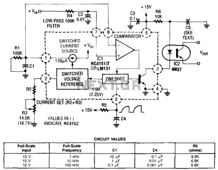
In this circuit, a Raytheon RC4151 or National LM131 is utilized alongside an optocoupler for applications where input-to-output isolation is desirable. Circuit values are indicated in the figure for various applications. The circuit employs a Raytheon RC4151 or National LM131,...

This circuit functions as a universal decoder, capable of operating either as a dual 1-of-4 decoder or as a single 1-of-8 decoder, depending on the signal applied to the Mode Control (M) input. In the dual mode, each section...
The schematic shows R4 at the emitter of the transistor, as suggested by Amb and Majkel. It should be positioned between the operational amplifier and the transistor, which is also the correct configuration in the CanAmp. The amplifier observed...
Power line fluctuations and cut-offs can damage electrical appliances connected to the line, particularly domestic appliances such as refrigerators and air conditioners. When a refrigerator operates at low voltage, excessive current flows through the motor, leading to overheating and...
Many circuits can be powered directly from the mains with the aid of a series capacitor (C1). The disadvantage of this approach is that usually only one half cycle of the mains waveform can be used to produce a...
The timing circuit utilizes an electronic switch composed of F1, F2, and VT1 to reduce quiescent current to approximately 1 to 2 A with the 555 timer. Upon initial power-up, the voltage across capacitor C2 cannot instantly change, causing...