
Pulse-Width Modulator
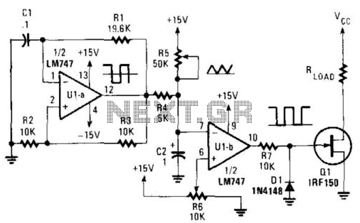
This circuit is an example of a pulse-width modulation (PWM) controller, which is commonly used in various applications for power management and control. The core component, U1A, is configured as an integrator, converting the square wave input into a triangular waveform. The integration process takes place over time, where R4 and C2 determine the frequency and amplitude characteristics of the triangular wave.
The comparator's role is crucial, as it compares the triangular wave against the adjustable reference voltage provided by R6. This comparison yields a PWM signal whose duty cycle is directly influenced by the value of R6. As the reference voltage is increased, the comparator will produce a narrower pulse width, resulting in reduced power delivered to the load. Conversely, decreasing the reference voltage will widen the pulse, increasing the load power.
Transistor Q1 acts as a switch controlled by the PWM signal. It modulates the current flowing to the load in accordance with the duty cycle of the PWM signal, allowing for precise control over the load's power consumption without significant energy loss in the switching components.
Resistor R5 serves to set the baseline or offset of the triangular wave generated across capacitor C2, ensuring that the waveform remains within the operational limits of the comparator. This offset adjustment is important for maintaining stable operation and avoiding unwanted oscillations or instability in the PWM output.
Overall, this circuit design illustrates an efficient method for controlling power in a load with minimal energy loss, making it suitable for applications such as motor speed control, light dimming, and other scenarios where variable power delivery is essential. This circuit allows the effective power in a load to be controlled by varying the duty cycle of the on/off ratio of l oad current. No power is dissipated in the switching circuit. U1A generates a bipolar square wave that is integrated into a triangle by R4 and C2. Reference voltage from R6 is fed to a comparator. The triangle wave on C2 goes to the comparator as well. By varying the reference voltage (R6), the output waveform is a variable width pulse, that drives Ql. R6 controls on/off ratio and therefore load power. R5 sets the offset of the triangle wave across C2. 🔗 External reference
Related Circuits
MC44BS374CA: PLL Tuned UHF and VHF Audio Video High Integration Modulator MC44BS374CA The MC44BS374CA Audio and Video Modulator is for use in VCRs, set-top boxes, and similar devices. By Freescale Semiconductor, Inc The MC44BS374CA is a highly integrated audio and...
The circuit receives a 32.768 kHz infrared (IR) input and produces a logic low output when the input signal is detected. The design consists of three distinct stages: the section up to U1A, the section between U1A and Q3,...
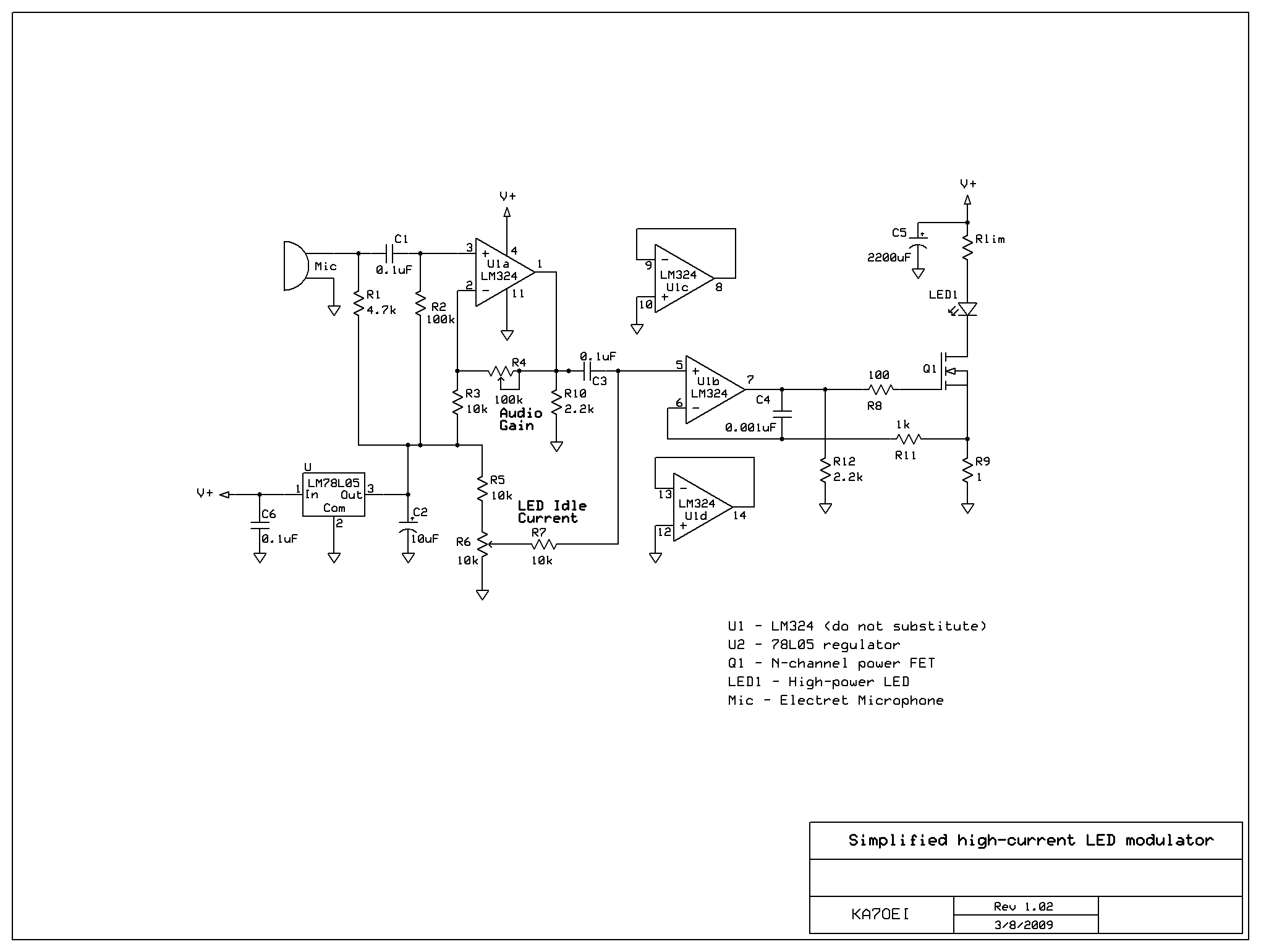
After constructing a Pulse Width Modulator for high-power LEDs, another LED modulator was developed for an optical transceiver. This project utilized a different approach, focusing solely on linear techniques for audio modulation. Similar to the PWM circuit, this circuit...
The circuit presented here enables amplitude modulation and offers the significant advantage of replacing the somewhat exotic and complex components typically required. This circuit is designed to implement amplitude modulation (AM) effectively, which is a technique used to encode information...
This circuit is designed to multiply the width of incoming pulses by a factor that can be either greater or less than one. It is straightforward to construct and features a single potentiometer for adjusting the multiplying factor. The...
Designing various electronic circuit systems (synthesizer, modem, decoder, data converter, etc.) often requires a frequency modulator subsystem. An FM modulator is a crucial component in these systems. An FM modulator is an electronic device that encodes information in a carrier...