
PWM Lamp or Motor Controller

This dimmer circuit is designed to control a 12V load, providing flexibility for both lighting and motor applications. The core of the circuit employs a pulse-width modulation (PWM) technique to regulate the power delivered to the load. The oscillator, formed by two inverter gates, generates a square wave signal whose duty cycle can be varied. This modulation allows for smooth dimming of the lamp or precise speed control of a motor.
The FET (Field Effect Transistor) acts as a switch that is controlled by the PWM signal. When the PWM signal is high, the FET turns on, allowing current to flow to the load. Conversely, when the PWM signal is low, the FET turns off, cutting off the current. The ability to vary the pulse width effectively controls the average power delivered to the load, resulting in dimming or speed control.
The veroboard layout is practical for prototyping and provides a straightforward method for assembling the circuit. The panel mounting of the potentiometer and FET not only facilitates user interaction but also enhances thermal management by allowing the FET to dissipate heat into the panel. The use of screw terminals simplifies the connection of power wires, ensuring a secure and reliable interface.
The design consideration for the 1N4148 diodes, which are used for flyback protection in motor applications, highlights the attention to detail in ensuring circuit reliability. By allowing the diodes to share a single hole for the common connection, the design minimizes space requirements on the board while maintaining functionality.
The transition to an etched PCB layout indicates a progression towards a more refined and durable version of the circuit. Utilizing a connector block with a 4mm pitch enhances the ease of connection and disconnection of the circuit, which is particularly beneficial in applications where frequent adjustments or replacements are necessary. The PCB design, presented at 600 dpi, ensures clarity and precision in the layout, making it suitable for manufacturing and assembly.This is another design generated at the request of my father. It is designed to be a dimmer for a 12V reading lamp, but could also be used as a motor speed controller (for a drill). The circuit pulse the voltage seen by the load an the pulse width is variable across the entire range from 0 to 100% (i.
e. from off to fully on). The circuit is extrem ely simple, using 2 inverter gates as an oscillator, and the remainder in parallel to drive the FET. The circuit schematic is: Because the circuit is simple, and I only wanted one of them, I didn`t think it was worth making an etched PCB, so a veroboard layout was produced. The layout below is intended to be mounted to a panel using the potentiometer thread and has screw terminals for the power wires.
The FET will also be mounted on the panel so that some heatsink effect can be gained from the panel. To allow this, and easy access to the screw terminals, both the Potentiometer and FET are mounted on the track side of the board. The Potentiometer is mounted in contact with the board and also glue is applied to keep it in place. The leads of the FET are bent up as shown and it is soldered in place so it is flat on the back of the panel.
As the leads of the 1N4148 diodes are so small, they share a single hole for the common connection. If you want to reverse the direction of operation of the potentiometer, just reverse both diodes from that shown. I later decided that an etched PCB was worth the trouble and created the following layout, which is intended to use a connector block with a 4mm pitch.
The PCB shown is at 600 dpi and shown looking from the track side. 🔗 External reference
Related Circuits
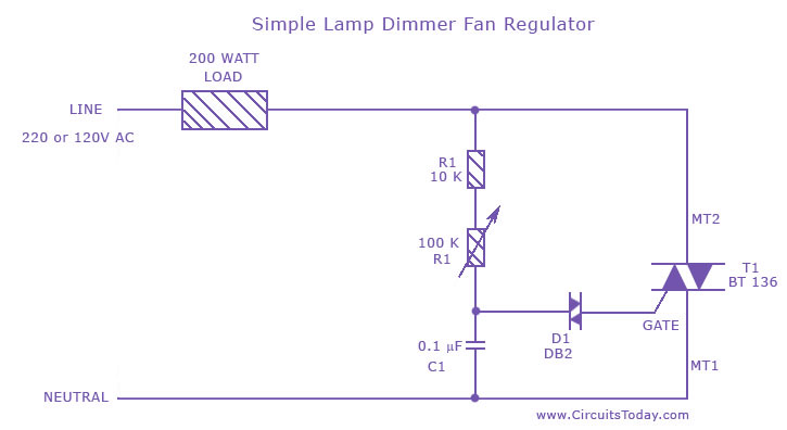
A fan regulator circuit that can also function as a simple lamp dimmer circuit. This fan speed regulator or light dimmer operates based on power control using a triac. The fan regulator circuit is designed to control the speed of...
This PC fan controller circuit is designed with discrete components to control 12V fans that consume less than 200mA. The specified component values in the circuit diagram ensure that the voltage will not drop below 7V. If the fan...

This circuit is essentially an 8W inverter circuit designed to drive an 8W fluorescent lamp from a 12V power supply. It utilizes an inexpensive inverter based on a ZTX652 transistor. The inverter will operate efficiently to convert the DC...

The Spartan-3an board features external interfacing for stepper motors, as illustrated in the accompanying figure. The stepper motor is driven by the ULN2803A, which is a high-voltage, high-current Darlington transistor array. The ULN2803 serves as a driver for the...

Voltage regulator ICs (78xx series) provide a steady output voltage, in contrast to a widely fluctuating input supply, when the common terminal is grounded. The 78xx series of voltage regulator integrated circuits (ICs) are widely utilized in electronic circuits to...
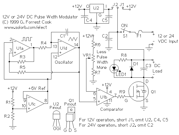
The circuit described here is for a general purpose device that can control DC devices which draw up to a few amps of current. The circuit may be used in either 12 or 24 Volt systems with only a...