
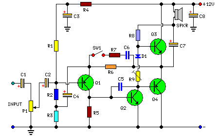
pwr amp

This circuit exemplifies innovative engineering, blending classic design principles with unique adaptations to achieve low distortion and high fidelity in audio amplification. The use of complementary LTPs and careful biasing strategies contribute to its distinctive performance characteristics, making it a noteworthy design in the evolution of audio amplification technology.This is an unusual circuit for an ultra-low distortion power amp. According to my original notes the circuit is dated January 1977 so the circuit is not exactly modern but it is still sufficiently different to be interesting. The circuit was designed and sold as a card by a purveyor of surplus components but, even using mostly manufacturer`s rejec
ted transistors, we managed to get about 0. 02% total harmonic distortion at 30 watts with a ±25v power supply into 8 ohms. : no bad figure even in these days of MOSFET and ICs. In 1977 anything below 0. 1% was considered excellent. And this figure was pretty repeatable without doing much selection. The problem of course is that since I haven`t touched this amplifier for many a year I have absolutely no idea what modern transistor types one should use for it but they are not critical: output transistors and drivers need to be the correct type but the other transistors can be small signal types - as long as they can handle the full voltage between + and - supplies. Tr1 and Tr2 are a long-tailed pair (LTP to save typing). It is quite common to have a LTP in an audio amp but this is different: this is a complimentary LTP. As far as I am aware no one else had used a complimentary LTP at the time, though I have since seen it used in one other circuit.
So I guess the circuit is unique to the author. One of the things that limits the performance of a conventional LTP is that the tail source loads the common emitters. In a complementary LTP this can`t happen as there is no tail current source so that all the current of one transistor has to flow through the other.
Tr2`s collector current flows into D1 and D2 which develop a voltage: this is used to bias Tr8 as a constant current source for Tr4`s collector. The fact that Tr4 is working at a constant current defines its base-emitter voltage which must be developed across R4.
This defines a current in R4 and this is the current that the LTP must operate at - so the ring of four transistors (Tr1, 2, 3, & 4) is self biasing and all transistors work at their best with minimum unwanted loads and biasing detracting from the performance. Tr4 is actually one of the most critical transistors: in the original circuit it was selected for Vce greater than 75v.
Most Texas BC212s passed easily. Lower voltage transistors caused an increase in distortion level. There is always a down side to any circuit: in the conventional LTP the base-emitter voltages tend to cancel each other out. In the complimentary LTP they add so there is a drop of about 1. 2v between the two bases: this must be cancelled in the biasing chain and, since this circuit was designed for operation over a wide range of supply voltage, I had to be a little clever.
Because of the constant current operation of the LTP and the constant voltage drop across D1 & D2, there is also a constant voltage across R14. This drop is used to lift up the bottom of the biasing chain (R1 and R11) so that the output sits at around half supply voltage, over a wider supply range.
The output transistors are complimentary (the original design used MJE2011 and MJE2021) and are driven by complimentary drivers: PNP driving NPN and vice versa. This arrangement is not only pleasingly symmetrical but gives better performance that the more common Darlington arrangement - the full gain of all the transistors is used and there is more internal feedback and less voltage drop.
The output current is monitored in the two resistors R7 and R22 (180 milliohms). The current limiting is unusual in that it works inside the input ring at an earlier stage than normal. This has an advantage that the current limiting transistors do not load the drive circuitry - which will introduce distortion.
The slight down side is that there may be a slight tendency to oscillation when in current limit. R3 and R14 are necessary to restrict the current availability when the current limit en 🔗 External reference
Related Circuits
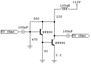
A 3KHz-50MHz signal generator is available, and there is a requirement to amplify its 2.3mW output to +7dBm. The need is for a broadband amplifier capable of achieving this amplification. To amplify the output of a signal generator from 2.3mW...

A MOSFET is employed to drive a load that includes a sense resistor in its current path. The voltage across this resistor is utilized to trigger a circuit capable of disconnecting the load in the event of an overcurrent...
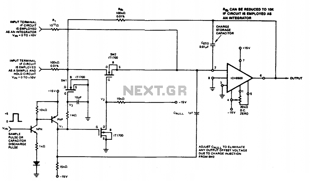
This circuit quickly charges capacitor CST0 to a voltage that matches an input signal. After charging, the input signal is electrically disconnected from the capacitor, allowing the charge to remain on CST0. Since CST0 is part of the negative...
This amplifier is designed to be self-contained within a compact loudspeaker enclosure. It can be powered by devices such as Walkmans, Mini Discs, iPods, CD players, computers, and other devices equipped with line or headphone outputs. Typically, two units...
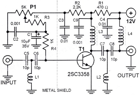
This HD TV UHF wideband amplifier (Ultra High Frequency amplifier) provides a total gain of 10 to 15 dB within the frequency range of 400 to 850 MHz, making it suitable for areas with weak TV signals. To ensure...
The LM317 integrated circuit (IC) is commonly recognized as an adjustable voltage regulator. However, it also has the capability to function as an audio amplifier, specifically in Class A configurations. The LM317 can be utilized in audio amplification applications due...