
Sample and hold circuit II
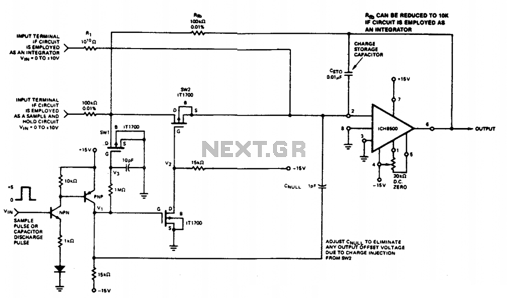
The described circuit primarily functions as a sample-and-hold circuit, utilizing an operational amplifier in a negative feedback configuration. The capacitor CST0 plays a crucial role in maintaining the voltage level that corresponds to the input signal, ensuring that the output of the amplifier remains stable during the hold phase. The operational amplifier, specifically the ICH8500A, is chosen for its minimal bias current, which is essential for maintaining low drift in the output voltage.
In the hold mode, the solid-state switch SW2 disconnects the input signal, allowing the charge on CST0 to be preserved. The design accounts for various leakage paths that could affect the performance, including the inherent leakage resistance of the capacitor itself and any parasitic resistances in the circuit layout. To mitigate these effects, careful PCB design practices should be employed, including short trace lengths and the use of high-quality components.
When utilized as an integrator, the circuit can integrate the input voltage over time, with the output reflecting the accumulated value. The time constant, dictated by the resistor Rl and capacitor Cg, is a critical parameter that determines the response time and stability of the integration process. This versatility makes the circuit suitable for a range of applications, including analog signal processing and data acquisition systems, where accurate voltage representation and stability are paramount.
Overall, the design emphasizes low drift and high accuracy, making it ideal for precision applications in electronic instrumentation and control systems.This circuit rapidly charges capacitor CST0 to a voltage equal to an input signal. The input signal is then electrically disconnected from the capacitor with the charge still remaining on CSTO. Since CST0 is in the negative feedback loop of the operational amplifier, the output voltage of the amplifier is equal to the voltage across the capacitor.
Ideally, the voltage across CST0 should remain constant causing the output of the amplifier to remain constant as well. However, the voltage across CST0 will decay at a rate proportional to the current being injected or taken out of the current summing node of the amplifier.
This current can come from four sources: leakage resistance of CST0, leakage current due to the solid state switch SW2, currents due to high resistance paths on the circuit fixture, and most important, bias current of the operational amplifier. If the ICH8500A operational amplifier is employed, this bids current is almost non-existent (less than O.OlpA).
Note that the voltages on the source, drain and gate of switch SW2 are zero or near zero when the circuit is in the hold mode. Careful construction will eliminate stray resistance paths and capacitor resistance can be eliminated if a quality capacitor is selected.
The net result is a low drift sample and hold circuit. The circuit can double as an integrator. In this application the input voltage is applied to the integrator input terminal. The time constant of the circuit is the product of Rl and Cg
Related Circuits
A circuit that activates a relay upon detecting audio pulses from one channel of an MP3 player. The intention is to synchronize recorded audio pulses with music to control a motor for mouth movement. For a stereo player, music...
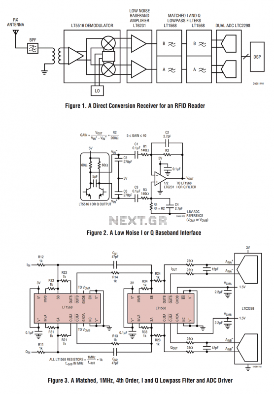
Figure 1 shows the block diagram of a direct conversion RF receiver—the receiver demodulates an RF carrier directly into a baseband signal without an intermediate frequency down-conversion (a zero IF receiver). The antenna, shared by both the transmitter and...
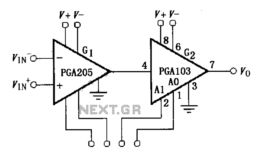
The circuit depicted in the figure comprises a PGA103 programmable gain instrumentation amplifier. This design utilizes the PGA205 and PGA103 in a cascading configuration, resulting in a total gain for the amplifier. The gain is determined by the product...
This schematic is directly sourced from the Altera ByteBlaster datasheet or manual, which provides comprehensive details regarding the connector's functionality and pin connections. It is advisable to review the datasheet available on their website or through a search engine...
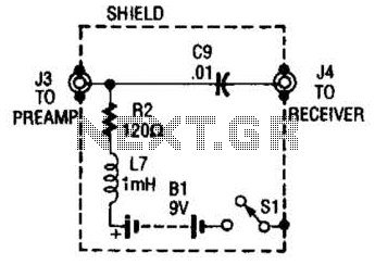
The purpose of the receiver/interface circuit is to pass RF to the receiver through capacitor C9, while adding DC power to the feedline through resistor R2 and RF choke L7. The receiver/interface circuit is designed to facilitate the transmission of...
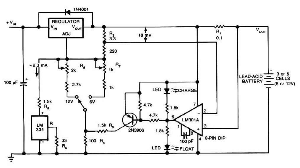
The schematic for this charger is straightforward. It is designed to charge a Gel Cell or other lead-acid types. This simple battery level monitor circuit can indicate the charging process in a 12 Volt lead-acid battery or tubular battery....