
QRP driver/final
The design of a simple 2 to 3W CW transmitter can be approached by integrating several key components to ensure functionality and efficiency. The transmitter will typically consist of an oscillator stage, a driver stage, and a final amplifier stage.
The oscillator stage is crucial for generating the carrier frequency. In this instance, a variable crystal oscillator (VXO) has been constructed for the 40m band. This VXO can be adjusted to fine-tune the output frequency within the designated band. The output from the VXO is usually a low-level signal that requires amplification for effective transmission.
The next stage is the driver amplifier, which takes the output from the VXO and increases its power level. A common choice for a driver stage in low-power CW transmitters is a transistor amplifier, which can be configured using a bipolar junction transistor (BJT) or a field-effect transistor (FET). The driver stage should be designed to provide sufficient gain while maintaining linearity to ensure clean signal transmission.
Following the driver stage, the final amplifier stage is employed to achieve the desired output power of 2 to 3W. This stage can be implemented using a power transistor capable of handling the required output power and providing good efficiency. The choice of transistor will depend on the operating frequency and the power handling capabilities. This stage must also include appropriate biasing to ensure the transistor operates in the desired region of its characteristics.
Additional considerations for the transmitter design include the implementation of a low-pass filter at the output to suppress harmonic frequencies and ensure compliance with regulatory standards. Adequate power supply decoupling and thermal management must also be addressed to ensure reliable operation.
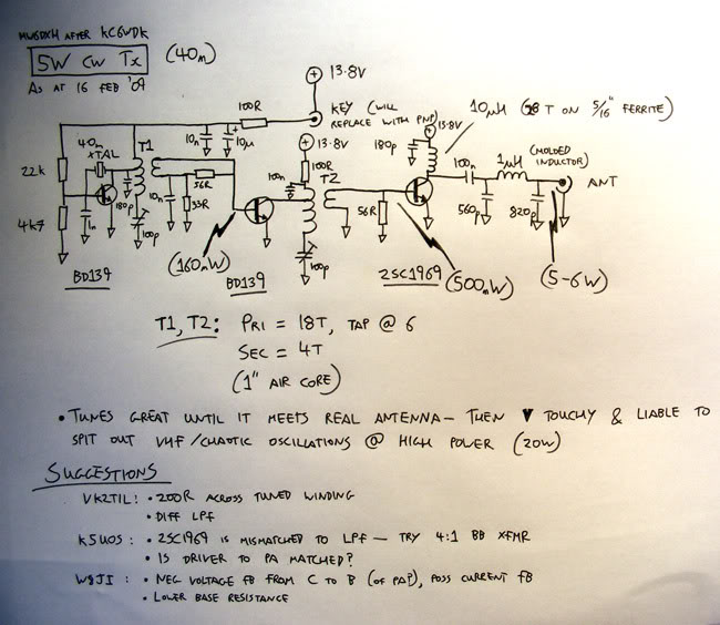
In summary, the construction of a simple CW transmitter involves a well-thought-out combination of an oscillator, driver, and final amplifier stages, along with necessary filtering and power management components. This project not only serves to enhance practical skills in electronics but also deepens the understanding of RF circuit design and operation.Hello all, I`m newly licensed last year but I`m kind of doing things the old way; getting heavily into CW and homebrewing. I`ve built a few simple receivers, an antenna matcher, SWR meter, PC-rig interface, and a kitbuilt 10W 80m SSB rig.
To further my understanding I`ve been trying to design a simple ""popcorn"" 2 or 3W CW transmitter based around bits in my junk box and it`s making me realise where the gaps in my knowledge are. I`ve made a 40m VXO. Now I`d like to add a driver, final.. 🔗 External reference
Related Circuits
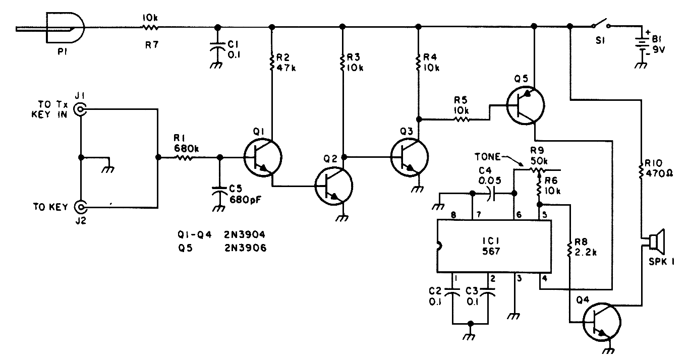
This circuit is designed for low-power transmitters that operate with a positive keying voltage. The transistors Q1, Q2, and Q3 are configured as a switching amplifier. When the key is pressed, the collector of Q3 connects to ground, which...
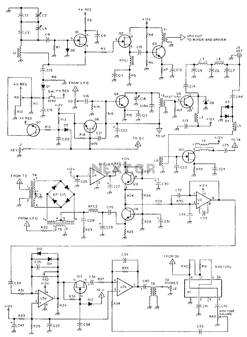
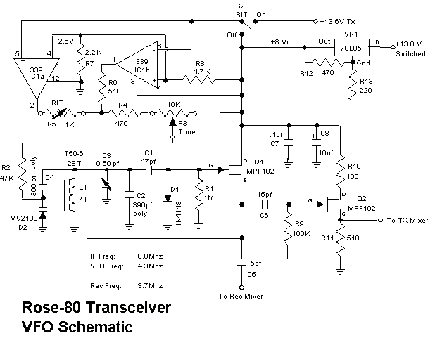
This is a 3-W, single-circuit board, VFO-controlled CW transceiver for 40 or 30 meters, featuring a direct-conversion receiver with audio filtering, Receiver Incremental Tuning (RIT), and speaker-level audio volume. The transmit frequency is generated by Q1 and its associated...
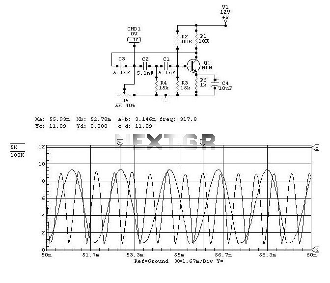
This project was a surprise as the BC547 transistor (equivalent to 2N2222) can be used to construct a 500mW linear amplifier that operates across the entire HF band with excellent spectral purity and without the need for neutralization. The...
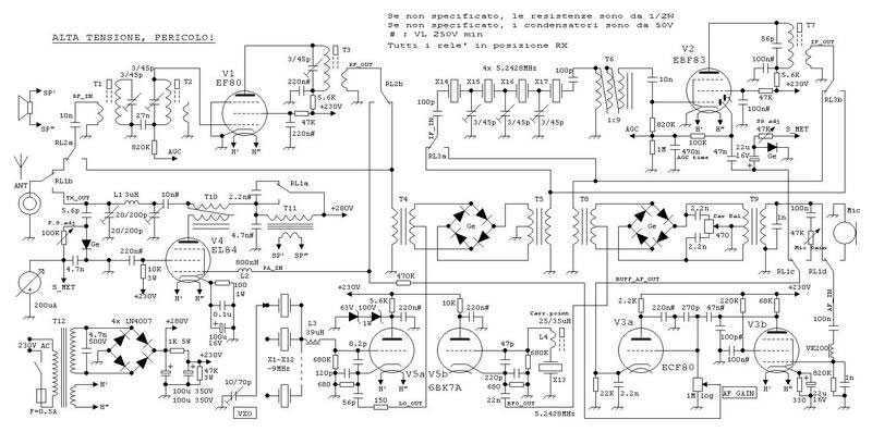
This true SSB transceiver is built around just 5 vacuum tubes, with no transistors nor ICs. Superhet receiver with AGC and S-meter drives a loudspeaker, 5W transmitter, very stable VXO uses CB crystals to cover 20m ham band. A...
1. Full 5 watt output using a power MOSFET final that is resistant to high SWR and thermal runaway. This final is very efficient and runs much cooler than traditional bipolar designs. 2. Highly sensitive and selective superhetrodyne receiver...
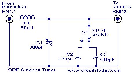
Low power (3 to 30 MHz) transmitters constructed by amateur radio operators are commonly referred to as QRP transmitters. A well-tuned antenna is essential for these transmitters; if the impedance is not properly matched, the output will be minimal...