
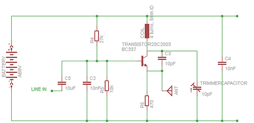
radionics schematics advanced
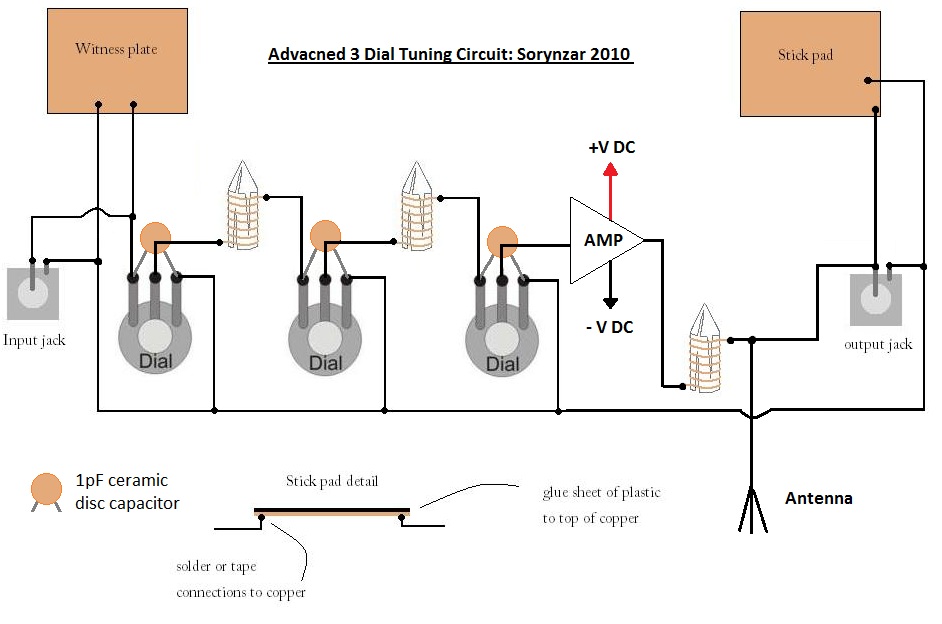
This schematic outlines a sophisticated approach to improving the efficiency and output power of a tuning circuit used in radionics applications. The circuit typically includes a combination of resistors, capacitors, inductors, and active components such as transistors or operational amplifiers. The primary goal is to optimize the resonance characteristics of the circuit, allowing for greater energy transfer and signal amplification.
Key components in the schematic may include:
1. **Resonant Circuit**: This is often formed by inductors and capacitors arranged to create a specific resonant frequency. The quality factor (Q) of the circuit can be adjusted by selecting appropriate component values, which influences the bandwidth and selectivity of the tuning circuit.
2. **Amplification Stage**: Utilizing transistors or operational amplifiers, this stage boosts the signal strength. The choice of components will affect the linearity and gain of the amplification process. Feedback mechanisms may be implemented to stabilize the gain and improve performance.
3. **Power Supply**: A regulated power supply is essential to ensure that the circuit operates efficiently. The power supply should provide a stable voltage and current to the active components, minimizing noise and fluctuations that could affect performance.
4. **Tuning Mechanism**: This can include variable capacitors or inductors that allow the user to fine-tune the circuit to the desired frequency. This adjustability is crucial for achieving optimal performance based on the specific application.
5. **Output Stage**: The final output stage may consist of a buffer or driver circuit that interfaces with the load. This stage must be designed to handle the required output power while maintaining signal integrity.
In conclusion, the advanced radionics schematic focuses on maximizing the power output of the tuning circuit by carefully selecting and configuring components to optimize resonance, amplification, and overall circuit efficiency. Proper implementation of this design can lead to significant improvements in the performance of radionics devices.An advanced radionics schematic to increase the power output of your tuning circuit.. 🔗 External reference
Related Circuits
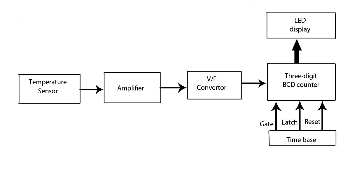
This verified project provides an idea, circuit, and operation of the LED display temperature indicator. It features a digital temperature indicator utilizing a voltage-to-frequency (V/F) converter, along with various electronic projects. The LED display temperature indicator is designed to provide a...
When working with these circuits, a light meter was purchased to eliminate the uncertainty in assessing light levels, as the human eye is not very reliable for this purpose. In electronic circuit design, particularly when dealing with light-sensitive applications, the...
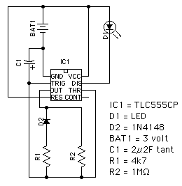
This circuit utilizes the TLC555CP timer integrated circuit to flash an LED approximately twice per second. This specific 555 timer operates on a voltage of only 3 volts, allowing it to be powered by two 1.5-volt cells. When using...
Utilize the program to customize your experience with the woven tules of roses on a single Adobe 3 Mac card. The system's reading portion remains idle while the controller operates, as illustrated in Figure 1. This setup includes the...
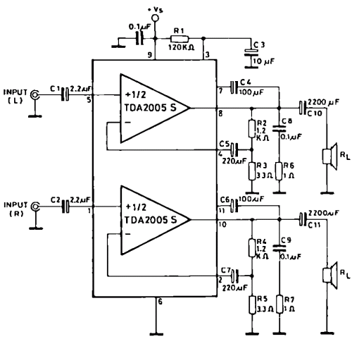
The TDA2005 integrated circuit (IC) features a high output power of 10W per channel (stereo) at a load of 2 ohms with a distortion of 10%, and 20W in bridge mode at a load of 4 ohms with a...
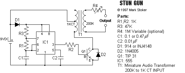
Instead of using a 555 timer integrated circuit, this design employs two transistors configured back-to-back to function as a multivibrator. This arrangement modulates the direct current sufficiently to traverse the magnetic field of a transformer. It represents one of...