
Random Access Memories
The static RAM (SRAM) architecture described is characterized by its efficient design, leveraging a six-transistor cell configuration that allows for stable data retention without the need for refresh cycles. The cross-coupled inverters serve as the core of the memory cell, providing the necessary feedback to maintain the stored state. Each SRAM cell can be accessed through a well-defined interface, where the control logic plays a crucial role in managing read and write operations.
The organization of the SRAM into an array format enhances its performance by minimizing the distance signals must travel within the chip, thereby reducing propagation delays. The use of row and column decoders further optimizes access time by enabling selective activation of memory cells based on the address provided. The structural design ensures that the data lines are shared among multiple cells, allowing for simultaneous reading and writing of data across the memory array.
In terms of application, the SRAM is suitable for high-speed data storage and retrieval tasks, often used in cache memory and other scenarios where rapid access to data is critical. The bidirectional data lines facilitate flexibility in operation, allowing the same physical connections to serve dual purposes, thus conserving chip space and simplifying the overall design.
The pin configuration, comprising address, data, and control lines, is designed to integrate seamlessly with various digital systems, ensuring compatibility and ease of interfacing. The active low Write Enable signal is a key feature that dictates the operational mode of the SRAM, allowing it to switch between read and write states efficiently.
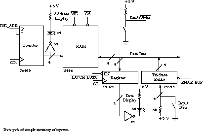
Overall, the design principles governing this 1024 by 4-bit SRAM exemplify modern memory technology's focus on efficiency, speed, and compactness, catering to the evolving demands of digital electronics.The memory system design: the detailed timing waveforms for a static RAM component, and the design of the register and control logic that surrounds the memory subsystem, making it possible to interface the memory to the rest of the digital system. But first, we must begin with the basics. We begin with a relatively simple memory component, a 1024 by 4-bit static RAM. The basic storage element of the static RAM is a six-transistor circuit, shown in Figure 7. 46. The "static" storage element is provided by the cross-coupled inverters. This circuit configuration will hold a 1 or 0 as long as the system continues to receive power. There is no need for a periodic refreshing signal or a clock. . To write the memory element, special circuitry in the RAM drives the data bit and its complement onto these lines while the word enable line is asserted. When driven in this fashion, the data bit can overwrite the previous state of the element. To read the contents of the storage element, the word enable line is once again enabled. Instead of being driven onto the data lines (also called bit lines), the data are "sensed" by a different collection of special circuits.
These circuits, called sense amplifiers, can detect small voltage differences between the data line and its complement. If Dataj is at higher voltage than RAMs are efficient in packing many bits into a circuit package for two reasons.
First, only a small number of transistors are needed to implement the storage elements. And second, it is easy to arrange these elements into rows and columns. Each row of memory cells shares a common word enable line. Each column shares common bit lines. The number of columns determines the bit width of each word. Thus, you can find memory components that are 1, 4, or 8 bits wide and that read or write the bits of a single word in parallel. Figure 7. 47 shows the pin-out for our 1024 by 4-bit SRAM (static RAM). The pins can be characterized as address lines, data lines, and control lines. Since the RAM has 1024 words, there must be 10 lines to address them. Since each word is 4 bits wide, there are four data lines. The same pins are used for reading or writing and are called bidirectional. The value on the active low control signal Write Enable ( ). When this signal goes low, a read or write cycle commences, depending on the value of write enable. If write enable is also low, the data lines provide new values to be written into the addressed word within the RAM.
If it is high, the data lines are driven with the contents of the addressed word. Internal Block DiagramFrom the preceding discussion, you might infer that the RAM is organized as an array with 1024 words and four columns. In terms of performance and packaging, this is not the best internal organization. A long thin array leads to long wires, which take more time to drive to a given logic voltage. Also, rectangular integrated circuits are more difficult to arrange on a silicon wafer for processing.
A square configuration is much more desirable. Figure 7. 48 gives a more realistic block diagram of the internal structure of a typical 1024 by 4-bit SRAM. The RAM array consists of four banks of 64 words by 16 bits each. This makes the array square. Let`s consider a read operation. The high-order 6 bits of the address select one of 64 words. Four groups of 16 bits each emerge from the storage array, one group for each of the possible data bits. The four low-order address bits select one of 16 bits from each of the four groups to form the 4-bit data word.
Writes are similar, except with data flowing in the opposite direction. This form of two-dimensional decode, with row and column decoders, is used universally in memory components. Not only does it keep the memory array square, it also limits the longest lines in 🔗 External reference
Related Circuits
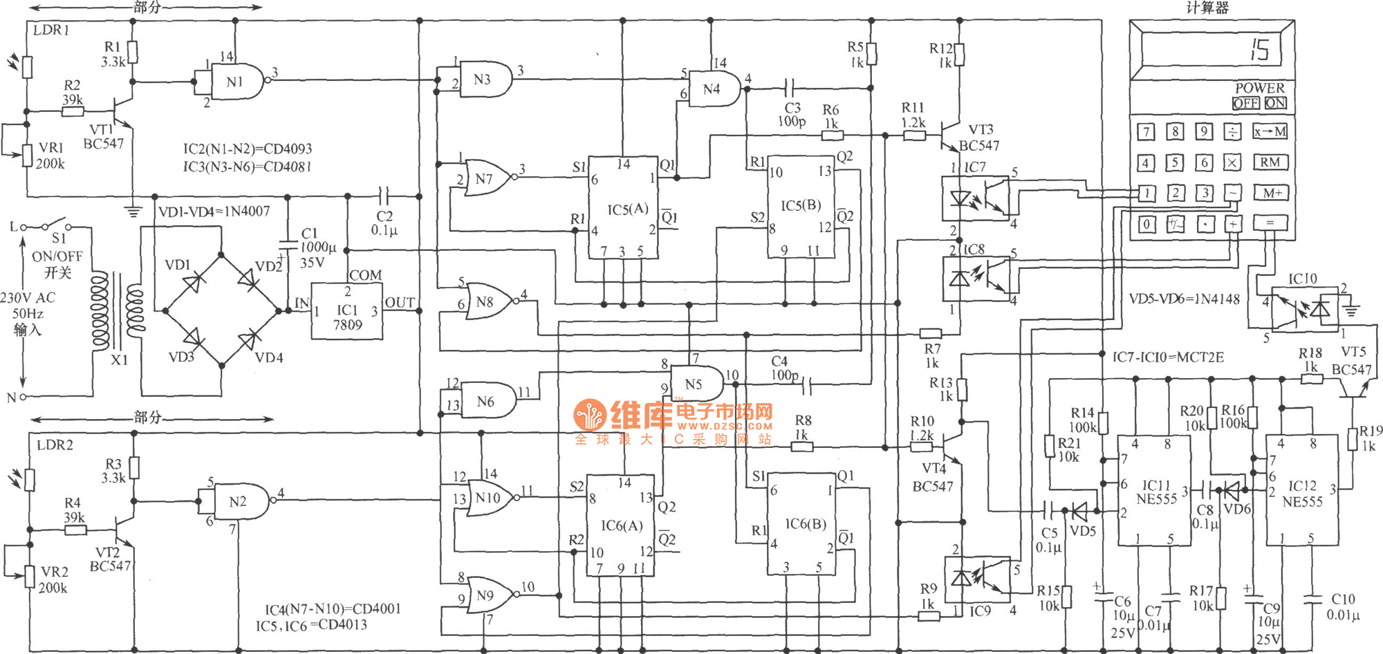
The working principle involves two pairs of photoelectric detection devices installed in the access channel. One side features light source A (transmitter) and photoresistor LDR1 (receiver) at the entrance of the channel, while the other side contains light source...
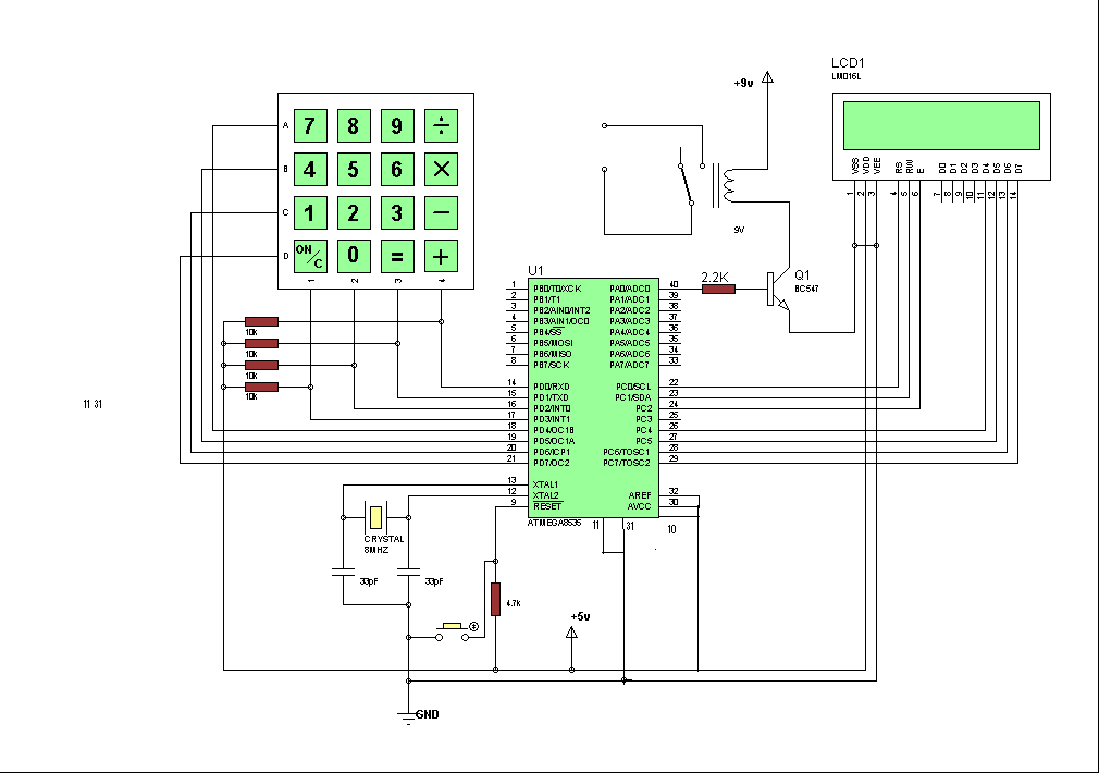
Security is a primary concern in daily life, and an access control system is a crucial component of a security framework. The microcontroller-based digital lock described here is an access control system that permits only authorized individuals to enter...
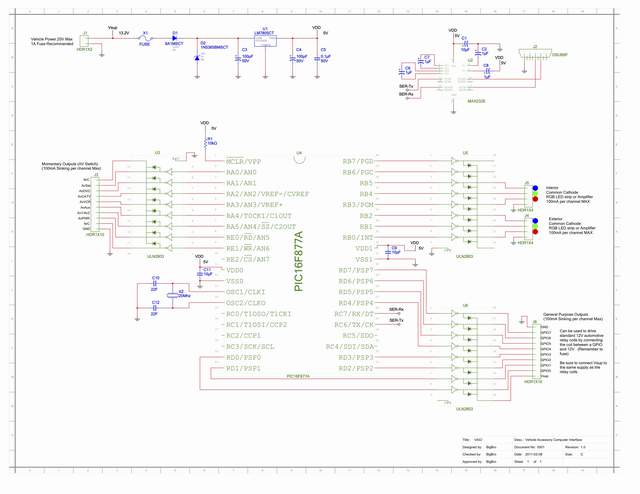
This document provides information for developing a Vehicle Accessory Computer Interface (VACI). The project involves a straightforward design that required approximately three weeks of planning, programming, and debugging. The interface has garnered significant interest, with many users expressing a...
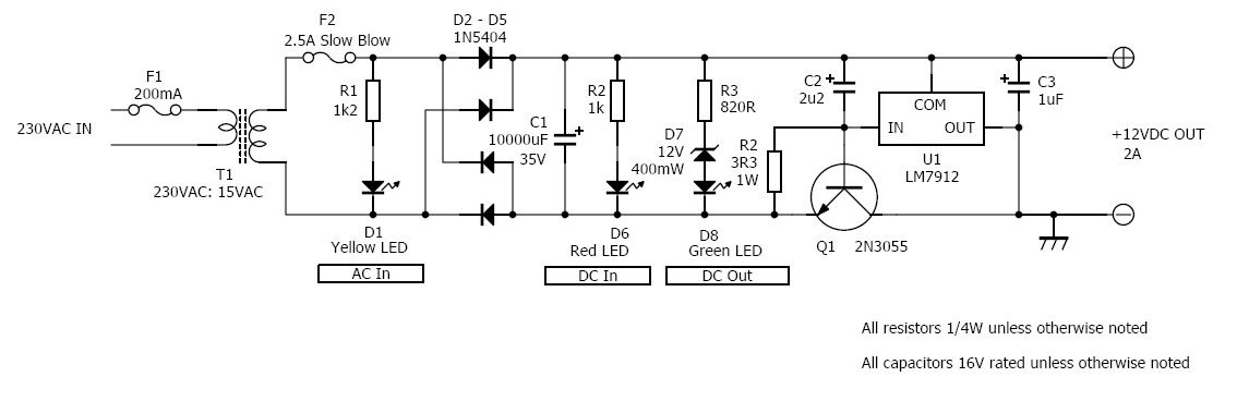
Accessories built so far include a linear power supply, a switch-mode power supply, a tuning aid, and a headset. An antenna tuner and SWR meter will be described later. To operate the new transceiver, a power supply was needed....
Much of the focus on residential gateway designs has been on distributing communication connectivity within a home. However, to effectively distribute content, gateways must first possess a reliable WAN interface that provides access to cable modems, fixed broadband wireless,...
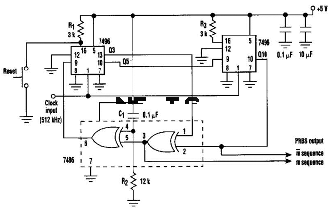
In this circuit, an additional exclusive-OR gate is connected after the modulo-2 feedback, with CI and R2 applying the supply turn-on ramp into the feedback loop. This provides sufficient transient signal so that the PRBS generator can self-start during...