
RC clock signal generating circuit
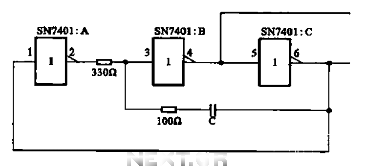
The clock signal generating circuit described employs a resistor-capacitor (RC) network to produce a stable clock signal, which is essential for synchronizing operations in TTL (Transistor-Transistor Logic) systems. The selection of the SN7401 series is significant due to its reliability and compatibility with TTL logic levels. The circuit is configured to utilize three inverters from this series, which can be connected in a feedback loop to create oscillation.
The frequency of oscillation is primarily influenced by the values of the resistor and capacitor used in the circuit. The relationship between the RC time constant and the resulting frequency can be expressed using the formula:
\[ f = \frac{1}{2 \cdot \pi \cdot R \cdot C} \]
where:
- \( f \) is the frequency in hertz (Hz),
- \( R \) is the resistance in ohms (Ω),
- \( C \) is the capacitance in farads (F).
For instance, with a capacitance value of 200 pF (picoFarads), the circuit can achieve a frequency of 5 MHz. Conversely, increasing the capacitance to 600 pF results in a reduced frequency of 1 MHz. This behavior is characteristic of RC oscillators, where increasing capacitance or resistance will lead to a decrease in frequency, while decreasing these values will increase the frequency.
The circuit layout will typically include connections for power supply, ground, and the output clock signal. Proper bypass capacitors should be employed near the power pins of the SN7401 inverters to ensure stable operation. Additionally, the resistor and capacitor should be chosen based on the desired frequency and the specific application requirements, taking into account tolerances and temperature coefficients for accuracy in timing applications.
Overall, this clock signal generating circuit is a fundamental building block in digital electronics, providing essential timing signals for various applications within TTL systems. As shown in the clock signal generating circuit as RC, which applies to most of the TTL system. This circuit requires only a 6-inverter set of circuit SN7401 three inverters. T he clock frequency depends on the value of RC, where C is the capacitance: C when 200 pF, the frequency of 5 MHz: C is 1 600 pF, the frequency of l MHz:
Related Circuits
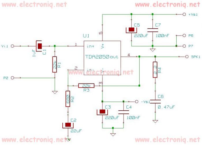
The TDA2050 integrated circuit can be used to design a simple high-fidelity audio power amplifier, intended for use as a Class AB audio amplifier. Due to its high power capabilities, the TDA2050 audio power amplifier can deliver up to...
The circuit designed for distortion measurements eliminates the fundamental frequency of 1 kHz, enabling the assessment of the residual harmonic levels. Initially, a true RMS meter is employed to measure the 1-kHz input level (E^) by positioning the switch...
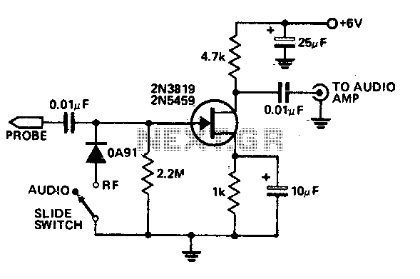
This economical signal tracer is useful for servicing and alignment work in receivers and low power transmitters. When switched to RF, the modulation on any signal is detected by the diode and amplified by the FET. A twin-core shielded...
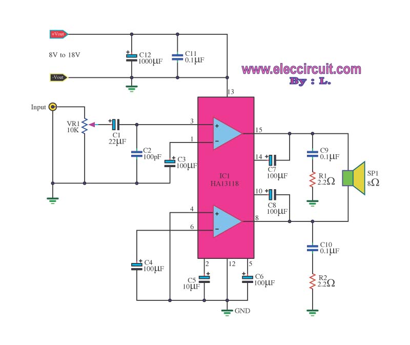
The amplifier circuit utilizes the HA13118 IC, a Hitachi component designed to deliver 18 watts of output power. This integrated circuit operates as a Class AB amplifier. The HA13118 IC is a versatile audio amplifier designed for high-fidelity applications, providing...
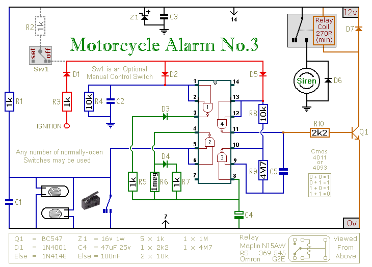
This circuit provides an intermittent siren output with an automatic reset feature. It can be operated manually through a key-switch or a hidden switch, and it can also be configured to activate automatically when the ignition is turned off....
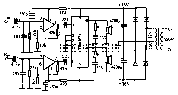
The first power amplifier circuit illustrated in Figure 5-88 utilizes the NE5532 operational amplifier, configured as a line amplifier, and features the TDA1521 power amplifier. This circuit operates with a dual power supply and eliminates the need for coupling...