
Receiver-Interface Circuit For Preamps Circuit
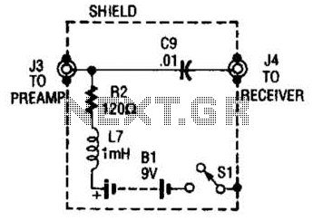
The receiver/interface circuit is designed to facilitate the transmission of radio frequency (RF) signals to the receiver while simultaneously supplying direct current (DC) power to the feedline. This is achieved through a combination of components: capacitor C9, resistor R2, and RF choke L7.
Capacitor C9 serves as a coupling element that allows RF signals to pass through while blocking any DC voltage. This ensures that the RF signal, which carries the information, can be effectively transmitted to the receiver without interference from the DC component. The selection of the capacitance value for C9 is critical, as it must be chosen to allow the desired frequency range of RF signals to pass while maintaining a high impedance to DC.
Resistor R2 is utilized to inject DC power into the feedline. This resistor is strategically placed to provide a path for the DC current while maintaining the integrity of the RF signal. The value of R2 must be carefully calculated to ensure that it does not excessively load the circuit, which could lead to signal degradation.
RF choke L7 plays a pivotal role in this circuit by blocking any RF signals from returning to the power supply while allowing the DC current to flow. This component is essential for preventing interference and maintaining the performance of the receiver. The inductance value of L7 should be selected based on the frequency of operation, ensuring that it effectively suppresses RF signals while allowing the desired DC current to pass through.
In summary, the combination of capacitor C9, resistor R2, and RF choke L7 creates an effective interface for the receiver circuit, enabling the passage of RF signals while simultaneously supplying necessary DC power to the feedline. Proper selection and configuration of these components are vital for optimal circuit performance. The purpose of the receiver/interface circuit is to pass RF to the receiver through capacitor 09, while adding dc power to the feedline through R2 and RF choke L7. 🔗 External reference
Related Circuits
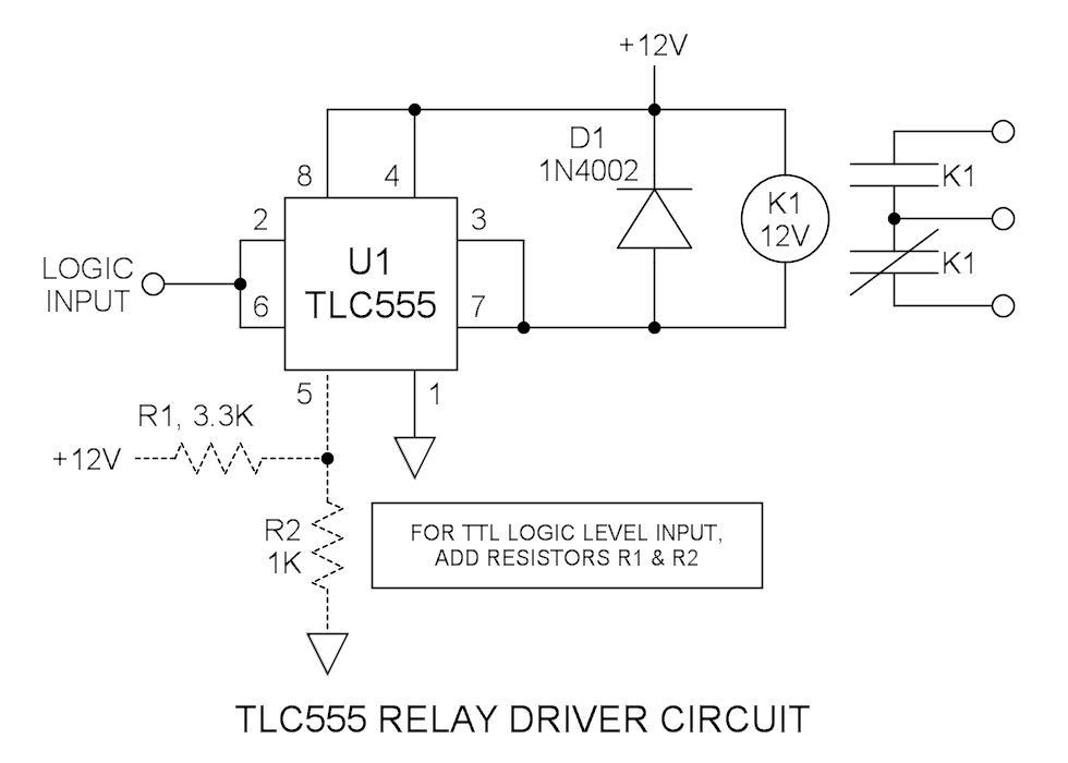
Many integrated circuits possess undocumented features or capabilities. The TLC555 output (pin 3) can sink a load of 100mA down to 1.28V. The open-drain transistor reset (pin 7) can also sink 100mA to 1V. Connecting both lines is permissible...

The LED meter circuit is more compact and simpler than its analog equivalent, making it a common choice in audio equipment. This circuit utilizes the LM3915 integrated circuit (IC) and operates in a logarithmic mode. It comprises a single...
Circuit Overview Many families now own various electronic devices such as televisions, VCD players, video recorders, game consoles, cameras, and DVDs. This circuit involves an RF signal repeater designed to work with a television signal transmitter, covering a radius...
Boiling water or cooking with a gas stove can sometimes lead to the fire being extinguished due to water spills, which can result in a significant gas overflow and pose a risk of poisoning. This example describes a stall...
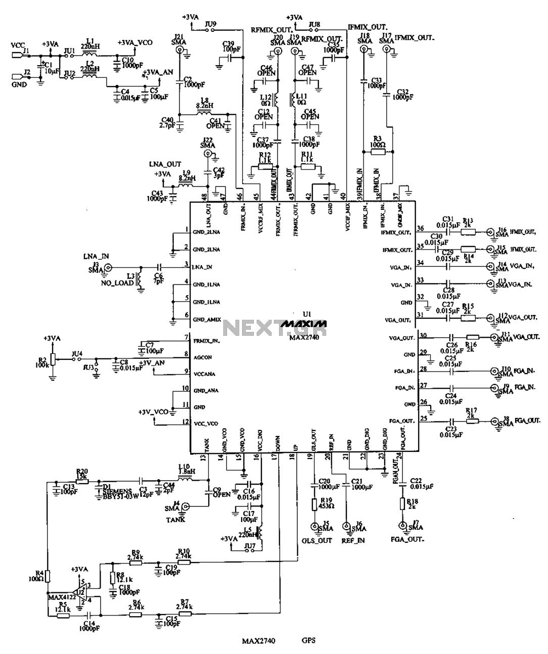
The MAX2740 is a complete GPS receiver down converter chip that processes the signal from the antenna to the input of digital signal processing. The receiver channel of the MAX2740 includes a low-noise amplifier (LNA), a downconverter, a variable...
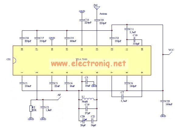
The TDA7000 features a Frequency-Locked-Loop (FLL) system with an intermediate frequency of 70 kHz, and selectivity is achieved through active RC filters. The only calibration required is for the resonant circuit associated with the oscillator, which is necessary for...