
Regulated 12 Volt Supply
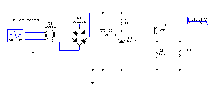
The circuit described operates on the principle of voltage regulation through the use of a zener diode in conjunction with a transistor amplifier. The 13-volt zener diode, D2, establishes a stable reference voltage. When the input voltage exceeds the zener breakdown voltage, the diode conducts and maintains the output voltage at approximately 12.3 volts after accounting for the voltage drop across the transistor's base-emitter junction.
The transistor serves to amplify the current capacity of the circuit, allowing it to deliver up to 500 mA to the load. This capability is essential for applications requiring a stable voltage supply for various electronic components. The configuration typically includes additional components such as resistors for biasing the transistor and capacitors for filtering to ensure stability and reduce noise in the output voltage.
In designing this circuit, careful consideration must be given to the selection of the zener diode and transistor to ensure they can handle the required voltage and current ratings. Additionally, heat dissipation mechanisms may be necessary, particularly if the circuit operates near its maximum load for extended periods, as both the zener diode and transistor can generate heat during operation. Proper thermal management will help maintain the reliability and longevity of the circuit.This circuit above uses a 13 volt zener diode, D2 which provides the voltage regulation. Aprroximately 0. 7 Volts are dropped across the transistors b-e junction, leaving a higher current 12. 3 Volt output supply. This circuit can supply loads of up to 500 mA. This circuit is also known as an amplified zener circuit. 🔗 External reference
Related Circuits
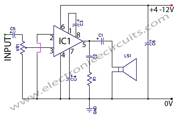
The LM386 is a power amplifier designed for use in low voltage consumer applications. The gain is internally set to 20 to minimize the need for external components. The LM386 power amplifier is a versatile component widely used in low-voltage...
Control a current through several current-mirror devices (specifically the IREF pin on the TLC5940) using a single potentiometer. A modified Howland current source has been utilized, which works adequately with the specified resistor values for dimming an LED. However,...
The circuit of the DC Voltage Doubler was designed for a specific type of power supply. It is important to study the schematic design and accompanying photographs of the DC Voltage Doubler circuit to understand the components involved. This...
This is a cost-effective circuit that incorporates precise current limiting functionality into a voltage regulator. The circuit described is designed to enhance the performance of a voltage regulator by integrating a current limiting feature. This is particularly beneficial in applications...
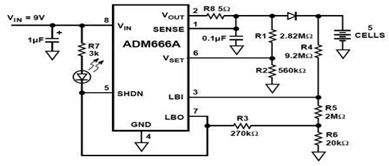
The ADM666A application note provides a detailed explanation of a low-cost battery charger circuit, including maximum output voltage, charge termination voltage calculation, battery voltage level monitoring, and circuit efficiency optimization. The ADM666A utilizes an NPN transistor and a P-channel...
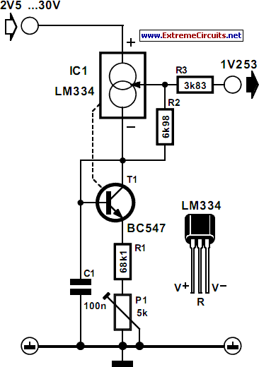
The current source IC Type LM334 is utilized in this specialized application, which features a minimal temperature coefficient and operates with a very low current draw of only 10 µA at room temperature. This current increases slightly with higher...