
Micropower Linear Voltage Regulator in the Battery Charger Circuit
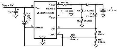
The ADM666A battery charger circuit is designed to provide an efficient and cost-effective solution for charging batteries in various applications. The maximum output voltage of the circuit is determined by the design specifications and the characteristics of the components used. The charge termination voltage is crucial for preventing overcharging, which can lead to battery damage. This is calculated based on the battery chemistry and desired charging profile.
Monitoring the battery voltage level is essential for maintaining optimal performance and longevity of the battery. The circuit includes a mechanism to continuously check the voltage at the LBI pin. If the voltage falls below the predetermined threshold of 1.3 V, the open-drain output (LBO) is activated, signaling that the battery is low. This output can be used to trigger additional actions, such as turning off the charger or alerting the user.
The circuit's efficiency is maximized by careful selection of the NPN transistor and P-channel FET, ensuring minimal power loss during operation. The use of a voltage divider allows for flexibility in setting the low battery threshold, accommodating different battery types and applications. Overall, the ADM666A provides a robust solution for battery management, integrating essential features for monitoring and charging with a focus on reliability and efficiency.In the ADM666A application note, you can find detailed explanation about this low cost battery charger circuit such as Maximum output voltage, Charge termination voltage calculation, monitoring the battery voltage level, maximizing the circuit efficiency, and etc. The ADM666A uses an NPN transistor and a P-channel FET. The output from the comparat or drives an open drain FET connected to the low battery output pin, LBO. The low battery threshold may be set using a suitable voltage divider connected to LBI. When the voltage on LBI falls below 1. 3 V, the open drain output LBO is pulled low. 🔗 External reference
Related Circuits
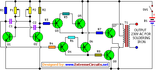
This is a simple and cost-effective inverter designed to power a small soldering iron (25W, 35W, etc.) when a mains supply is not available. The circuit utilizes eight transistors along with several resistors and capacitors. Transistors Q1 and Q2,...

The circuit depicted in Figure 3-99 illustrates a low start-up mechanism for a motor, which transitions to high-speed operation automatically. The start-up process is facilitated by a shaped connection, while the transition to high-speed operation is managed by a...
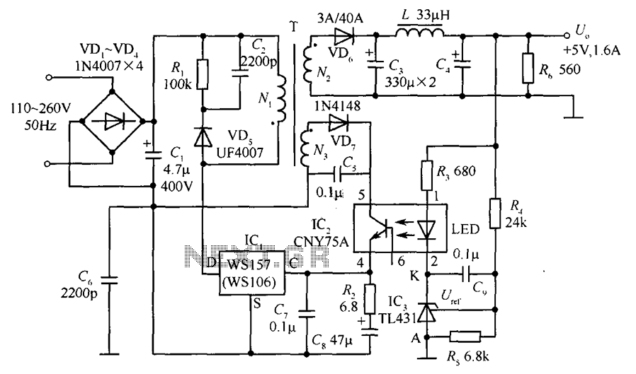
The circuit incorporates an optical coupler (CNY75A) and an adjustable precision shunt regulator (TL431). It includes current limiting resistors R3, R4, and R5 for the sampling resistor. As the output voltage (Uo) varies, the voltage across the sampling resistor...
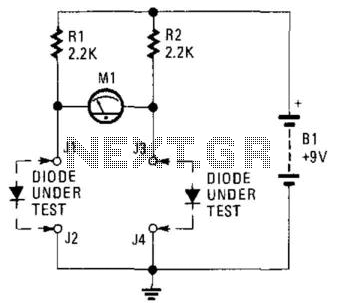
This circuit can be utilized to match diodes for applications where balance is essential, such as in a balanced modulator. The diode matching circuit will display the forward voltage drop of the two diodes in millivolts. The diode matching circuit...
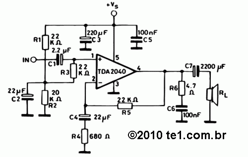
The TDA2040 is a monolithic integrated circuit housed in a Pentawatt package, designed for use as an audio class AB amplifier. It typically delivers an output power of 22W (with a distortion factor of 0.5%) at a supply voltage...
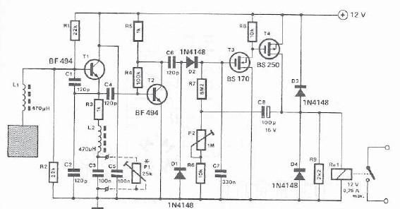
A simple proximity detector can be created using this electronic circuit. This circuit responds to the presence of a conductive object within a specific range. The sensitivity of the circuit can be adjusted with potentiometer P1 to achieve the...