
Regulated 12 Volt Supply
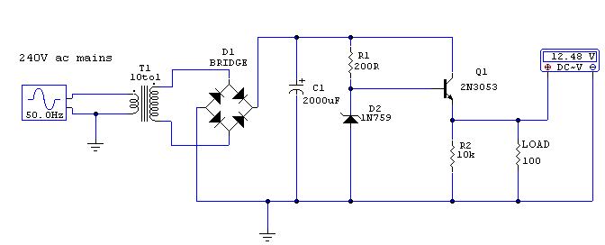
The amplified zener circuit is designed to provide stable output voltage regulation while allowing for higher current delivery compared to a standard zener diode configuration. The 13-volt zener diode (D2) acts as a reference voltage, ensuring that the output remains consistent despite variations in input voltage or load conditions.
The transistors in the circuit function as current amplifiers, which means they are capable of increasing the current supplied to the load while maintaining the desired voltage level. The base-emitter junction of the transistors introduces a voltage drop of approximately 0.7 volts, which is crucial for the operation of the transistors in the active region. This drop must be accounted for in the overall voltage output, leading to the effective output voltage of 12.3 volts.
The circuit's design allows for a maximum load current of 500 mA, making it suitable for various applications that require a stable power supply. The use of a zener diode for voltage regulation in conjunction with transistor amplification provides a robust solution for maintaining output voltage under different load conditions. This configuration is particularly useful in power supply circuits where consistent voltage levels are critical for the proper functioning of electronic components.
In summary, the amplified zener circuit is an effective voltage regulation solution that combines a zener diode with transistor amplification to deliver a stable output voltage capable of supporting moderate load currents. Its design principles can be applied to a variety of electronic applications requiring reliable power supplies.This circuit above uses a 13 volt zener diode, D2 which provides the voltage regulation. Aprroximately 0. 7 Volts are dropped across the transistors b-e junction, leaving a higher current 12. 3 Volt output supply. This circuit can supply loads of up to 500 mA. This circuit is also known as an amplified zener circuit. 🔗 External reference
Related Circuits
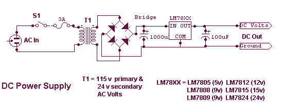
I didn't realize till the other day that I have never shown a circuit for a standard power supply. Shown below is a supply that will use any of the LM78XX series of voltage regulators. The transformer in the...
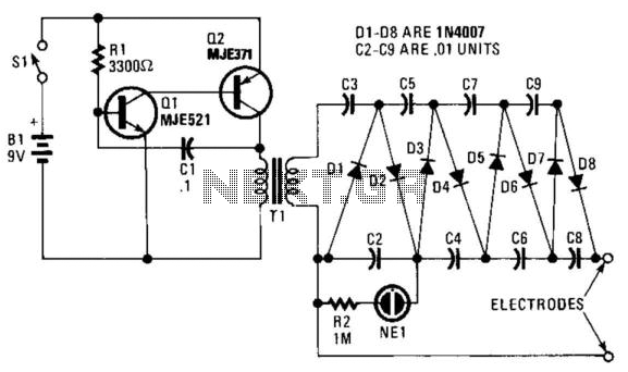
This circuit consists of components Q1, Q2, R1, and C1, which together create a multivibrator. The oscillation produced results in a square wave with a voltage peak-to-peak (Vpp) ranging from 20 to 30 volts. This output is then amplified...
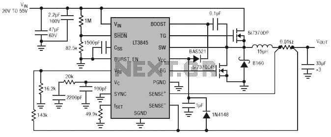
Burst Mode operation maintains high efficiency at light loads by reducing IC quiescent current to 120 µA. Light load efficiency is also improved with the reverse inductor current inhibit function, which supports discontinuous operation. Additional features include an adjustable...
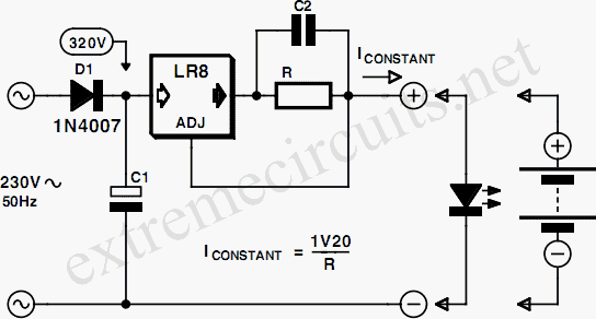
Commonly used 3-pin linear voltage regulators, such as the LM317, typically cannot handle input voltages exceeding approximately 30V. The LR8A from Supertex Inc is a new adjustable three-pin regulator that can accept input voltages up to 450V and can...
This circuit is designed for high current applications using nickel-cadmium rechargeable batteries, and it can also function as a general low-voltage DC power supply. The circuit consists of a charging section and a DC output section. K2 serves as...
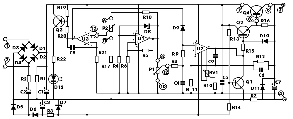
This is a high quality power supply with a continuously variable stabilised output adjustable at any value between 0 and 30VDC. The circuit also incorporates an electronic output current limiter that effectively controls the output current from a few...