
Reverse Engineering a 1.5 inch Photoframe

The electronic schematic of the described device can be organized into several key components: the TFT display, the control interface, the power supply, and the connections to the microcontroller. The TFT display, driven by the ILI9163, interfaces using an 8-bit data bus, which consists of eight data lines (DB0 to DB7) connected to corresponding GPIO pins on the microcontroller. The control lines include RESET, WR, RD, RS, and CS, each linked to specific GPIO pins, facilitating communication and command execution between the microcontroller and the display.
Powering the circuit involves a 3.7V Li-ion battery connected to the Vdd and Gnd pins of the display. The backlight is powered through the Anode and Cathode connections, allowing for illumination when required. The schematic should illustrate the power management, ensuring that the battery is protected from over-discharge and short-circuit conditions, possibly incorporating a battery management IC.
For the control logic, the microcontroller must be configured to handle the timing and signaling required for the display operation. This involves setting up registers for data transmission, as well as managing the read and write operations through the RD and WR lines. The RESET line must be utilized to initialize the display, ensuring it is in a known state before any commands are sent.
Overall, the schematic should represent a clear layout of the connections, including the necessary decoupling capacitors for power stability, and any additional components required for interfacing, such as pull-up resistors on the control lines if needed. This detailed schematic serves as a foundation for further development and experimentation with the repurposed photo frame displays.These little devices had a 1. 5 inch 128x128 colour TFT as well as USB, batteries and 16 Mbytes of storage for around 140 pictures. Best of all they were very cheap, so I purchased a few to see if they could be re-purposed into something useful.
Looking on ebay it seems these devices are common-place and it wouldn`t surprise me if most are internally identical Here is the box for one of the frames I bought: Out of the three I bought two had LCDs marked FTM144D01N and the other had the marking LC12802. 2, however both models looked functionally identical. The issue I found was that there was no available information on the display via Google, the only reference I found was that the FTM144D01N was based on the ILI9163 LCD driver IC from ILITEK.
Since I had more that one, I decided to leave one photo frame intact and remove the screen from the other. This would allow me to analyse the working frame whilst attempting to control the other on the breadboard.
Use a pair of side cutters to remove the Li-Po battery. Make sure you insulate the positive wire once cut so you don`t short the battery. The battery is a 3. 7V Li-ion 120mAh cell which is very useful for other projects. Next place the circuit board in a vice and use the wick to remove the excess solder. Simply heat the soldering iron to about 340C and then place the braid over the connector (partly on the board and partly on the ribbon) then apply the flat soldering tip for a short time to remove the solder. Once that`s done you hold the LCD in one hand and run the soldering iron across the ribbon whilst gently twisting the LCD free from the circuit.
The ribbon should come away easily. The first step to reverse engineering the LCD connections is to simply look at the connector itself. As can be seen in the following picture the ribbon has 27 connections of which many are simply not connected. I`ve marked the unused connections in red: The ruler placed under the ribbon shows that the connector is 22mm approximately.
This means that the connector pitch is 22/27 = 0. 81; this gives us a connector pitch of 0. 8mm (which is pretty typical for a display). From looking at datasheets for other similar ILI9163 based displays it can be seen that the LCDs are typically 8 or 16 bit parallel interfaces and have 5 control lines: RESET, WR, RD, RS and CS. In addition there are 2 power lines (Vdd and Gnd) and 2 power lines (Anode and Cathode) for the display backlight.
Using a multimeter on the working photo frames showed that pins 1 and 2 are Vdd and Gnd and that pin 26 was the backlight Cathode (positive) and 27 was the backlight Anode (negative). From the picture above you can also see that there are 8 pins which are all separated by unconnected pins, they also all go to the same group of tracks into the LCD.
From that you can easily infer that pins 10, 12, 14, 16, 18, 20, 22 and 24 are the DB0:7 data-bus. This means the LCD is a 8-bit parallel interface. This leaves 5 pins unaccounted for which (thankfully) matches with the expected number of control pins. The photo frame had a small reset button on the back so identifying the RESET line was as simple as pressing the reset switch and seeing which line dropped using an oscilloscope; this was pin 9.
Finding the rest of the control pins was a little more difficult, using just trial and error would take a long time. Since the ILI9163 data-sheet had some signalling diagrams I decided to compare the pins using a dual-channel oscilloscope to see if they could be identified.
Pin 7 was at a constant 3. 3Vs in the working photo frame so that was most likely the RD pin since that is the read/write selection (and the photo-frame only needs to write to the display). The data-sheet information showed that during operation the WR and CS lines would follow each other closely with the CS
🔗 External reference
Related Circuits
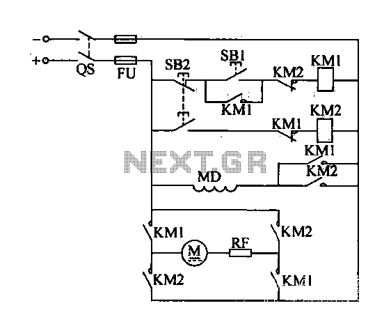
A DC motor reverse brake circuit is presented. To initiate braking, the stop button (SB2) is pressed, which disconnects the move-off contact, causing KM1 to lose power and release. Subsequently, the brake contactor (KM2) is activated. KM2 is designed...
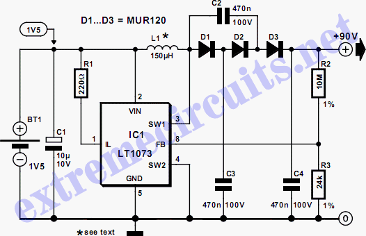
The circuit illustrates a method to obtain a voltage of 90V from a 1.5V battery supply. The LT1073 switching regulator from Linear Technology operates in boost mode and can function with an input voltage as low as 1.0V. The...
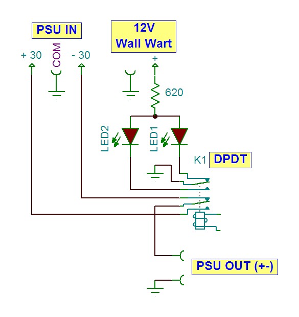
Thank you for the clarification. Since a dual (+-) supply is available, a single-pole double-throw (SPDT) relay will be sufficient. Is there a preference for a solid-state relay? A dual power supply configuration, typically indicated as +V and -V, allows...
The circuit depicted in Figure 3-146 eliminates the need for a step-down transformer by utilizing the principle of energy storage through capacitor discharge for braking. It can be employed to frequently start and stop a motor with a power...
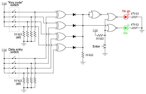
This experiment can be constructed using a single 8-position DIP switch, although utilizing two switch assemblies may facilitate a better understanding of the concept. One switch assembly is designated to hold the correct code for unlocking the lock, while...
The U2745B is a Phase-Locked Loop (PLL) transmitter integrated circuit (IC) designed specifically for low-cost radio frequency (RF) data transmission systems, supporting data rates up to 20 kBaud. It operates within a transmitting frequency range of 310 MHz to...