
RF-AMP Documentation
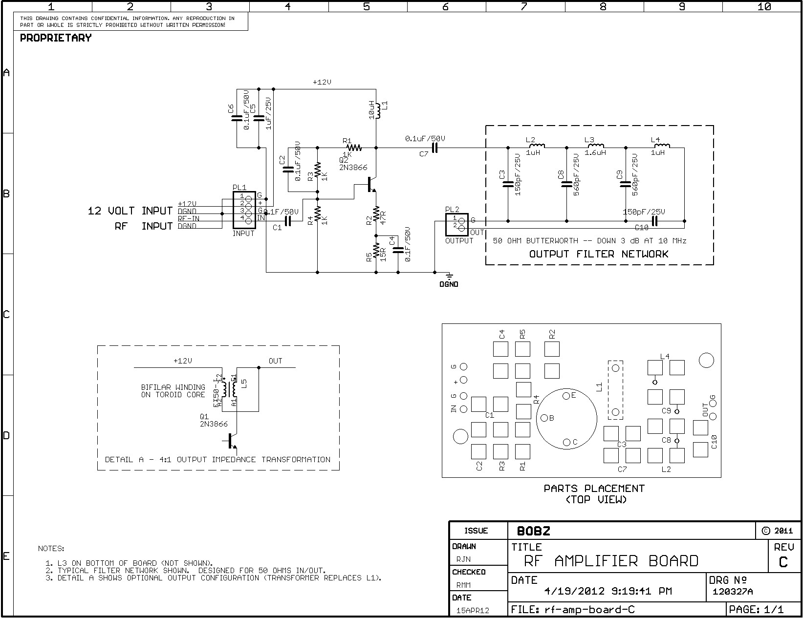
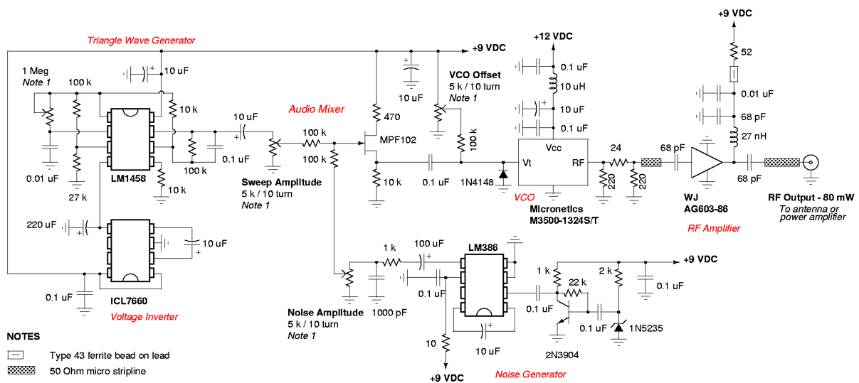
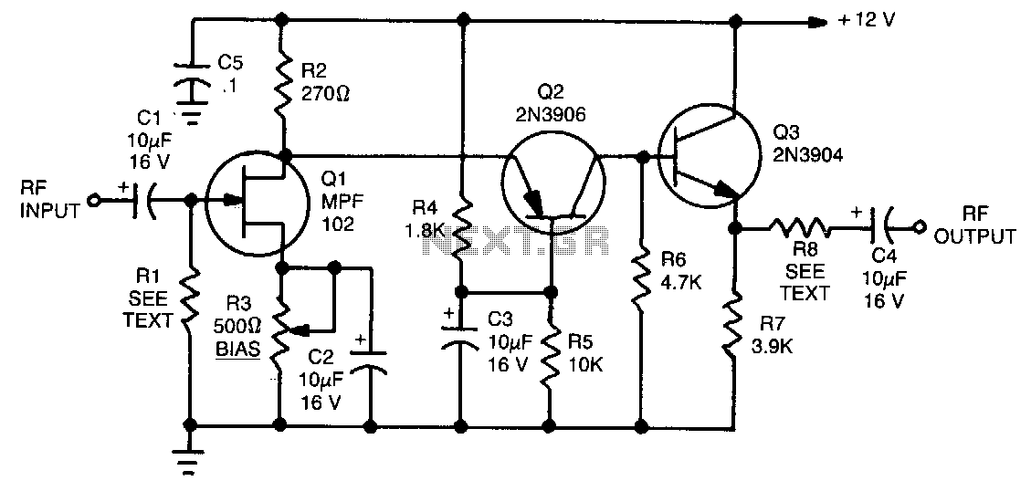
The amplifier circuit is designed to enhance signal integrity and performance in various applications, particularly in radio frequency (RF) systems. The use of the 9833 DDS chip as a signal source allows for precise frequency generation, making the amplifier essential for applications where signal fidelity is crucial. The incorporation of a bifilar wound 4:1 output transformer serves to match impedance and optimize power transfer between stages, significantly improving overall system efficiency.
The voltage gain specifications indicate that the amplifier is capable of providing a substantial increase in signal strength, which is critical in RF applications where weak signals must be amplified for further processing. The gain versus frequency plots illustrate the amplifier's performance across different frequency ranges, highlighting its suitability for both high-frequency and low-frequency applications. The distinction in output impedance under different configurations is important for ensuring compatibility with various load conditions, which can affect signal quality and amplifier stability.
The choice of core material in the transformer is vital for determining the amplifier's operational bandwidth. The FT50-J core is optimal for medium frequencies, while the type 43 core is recommended for higher frequency operations due to its superior magnetic properties. This attention to core selection ensures that the amplifier maintains performance across the intended frequency ranges, thus catering to a wide array of RF applications.
In summary, this amplifier circuit is a versatile solution for buffering and amplifying signals in DDS-based projects and Amateur Radio applications, demonstrating flexibility in design and robust performance across various frequency ranges.The amplifier can be used in a number of projects to buffer and amplify outputs from devices such as Direct Digital Synthesizer (DDS) chips. The board was initially produced to amplify the output of the 9833 DDS chip. The board was also intended for Amateur Radio applications (e. g. , a buffer amplifier for a VFO). Photo 1 shows the bare board and a board populated with all components except the optional output filter network. The board shown uses a bifilar wound 4:1 output transformer (as shown on the schematic and mentioned below). Schematic 1 shows the RF-Amp circuitry and a typical configuration of the optional output network. Note: with the given filter network, frequencies above 10 MHz are greatly attenuated. The schematic shows the board`s component layout, circuitry and connection points. The amplifier provides a voltage gain of approximately 16 to 18 dB. Photo 2 shows a gain vs. frequency plot of the basic amplifier board with an output optimized for the 3-10 MHz range (2000 Ohm load).
Shown on this plot are the results for three different transformer windings, as follows: Photo 3 shows a gain vs. load plot of the basic amplifier board for the three windings given above. These plots show that the output impedance of the amplifier is approximately 220 Ohms without the 4:1 winding.
With the impedance transformer, the output impedance is reduced to approximately 150 Ohms. The reduction over the 12 turn transformer is not 4:1 probably because the differences between the collector impedances for the two different transformers; the collector loading for the two transformers is comparable, but not exact. With the 4:1 transformer, a 2000 Ohm load and a frequency of 6 MHz, the voltage ratio between the collector and secondary of the transformer was (4220 mV rms)/(2210 mV rms)=1.
91. This is very close to the expected ratio of 2:1 (impedance transforms as the square of the voltage). Photo 4 shows a gain vs. frequency plot of an amplifier board optimized for operation at a lower frequency (e. g. , 300-400 kHz) connected with the optional 4:1 output transformer shown in the schematic. Photo 5 shows a load plot for the same low frequency amplifier. The output impedance, as determined by the point that the load reduces gain by one-half, is approximately 100 Ohms. Because the available supply voltage was only 11. 8 Volts for the low frequency plots, the gain will be somewhat larger with a full 12 Volt supply. Also note that the amplifiers use a FT50-J core, as noted. This core is good for operation at a few hundred kilohertz to several megahertz. For higher frequency operation, the type 43 core gives better results. 🔗 External reference
Related Circuits
Datagoo is based on the ATMEGA328P microcontroller, widely used by hobbyists in various Arduino projects. It can be programmed via any computer with a USB port when paired with an FTDI FT232RL USB-Serial circuit. Cost-effectiveness and simplicity were prioritized...
The following outlines the design, construction, operation, and use of the DECUS divider module. A top view of the module is depicted in Photo 2, while Photo 3 illustrates the bottom. The primary function of the module is to...
The use of a double-tuned input and a single-tuned output yields superior RF selectivity compared to equivalent single-tuned designs. Automatic Gain Control (AGC), if required, can be added to gate 2 of Q1 and should drive gate 2 negative...
Note that the due dates for lectures 20-25 will be rescheduled to Wednesday at 1:00 PM. Download the notes for Topic 1: Basic Components (Listen to Dr. Stienecker) and Topic 2: Power and Connections (Listen to Dr. Stieneker). Students...

The provided connections will enable configuration-free usage for most Arduino boards. Some Arduino boards, such as the Mega2560, may require custom configuration due to how the ports on the Atmel AVR microcontroller are mapped to the digital pins on...
The circuit features a frequency response ranging from 100 Hz to 3 MHz, with a gain of approximately 30 dB. Field-effect transistor Q1 is configured in a common-source self-biased mode. An optional resistor R1 allows for the adjustment of...