
RF Amplifier For FM 88-108 MHzCircuit With Double Transistor
The RF amplifier circuit operates within the FM broadcast band, which is crucial for applications such as radio transmission and reception. The BLV10 transistor, known for its high gain and low noise characteristics, is employed in this design to amplify weak radio frequency signals effectively.
The circuit typically includes a few key components: the BLV10 transistor, resistors for biasing, capacitors for coupling and bypassing, and an inductor or transformer for impedance matching. The input stage of the amplifier is configured to accept the incoming RF signal, which is then amplified by the BLV10. The output stage is designed to deliver a strong, clean signal to the next stage of the system or directly to the antenna.
Biasing resistors are critical in setting the operating point of the transistor, ensuring it functions in the active region for optimal amplification. Coupling capacitors allow the RF signal to pass while blocking any DC components, thus preventing interference with the amplifier's operation. Bypass capacitors are used to stabilize the voltage supply and minimize noise.
Impedance matching is also an essential aspect of the design, as it maximizes power transfer between the amplifier and the load, which can be an antenna or another circuit stage. This is often accomplished using a combination of inductors and capacitors configured in a matching network.
Overall, this RF amplifier circuit is designed for simplicity and efficiency, making it suitable for a variety of applications in the FM broadcast range. Proper layout and component selection are crucial to achieving the desired performance, ensuring minimal signal loss and distortion throughout the amplification process.The following circuit shows about RF amplifier for FM 88-108 MHz with no tune (broadband) Circuit Diagram. This circuit using the BLV10 & .. 🔗 External reference
Related Circuits
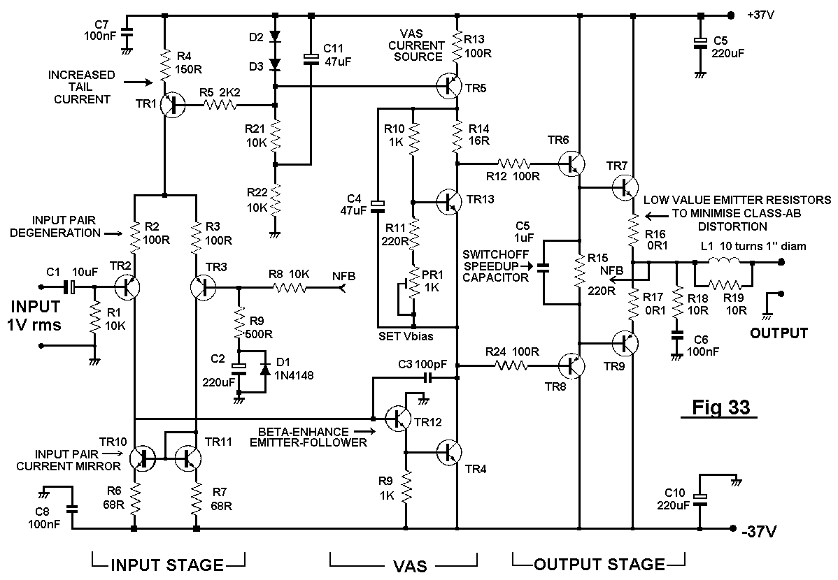
The distortion produced by a typical solid-state Class-B power amplifier consists of eight mechanisms, all of which may coexist and whose distortion products overlap to create a complex result. Methods for isolating each mechanism for study and minimizing its...
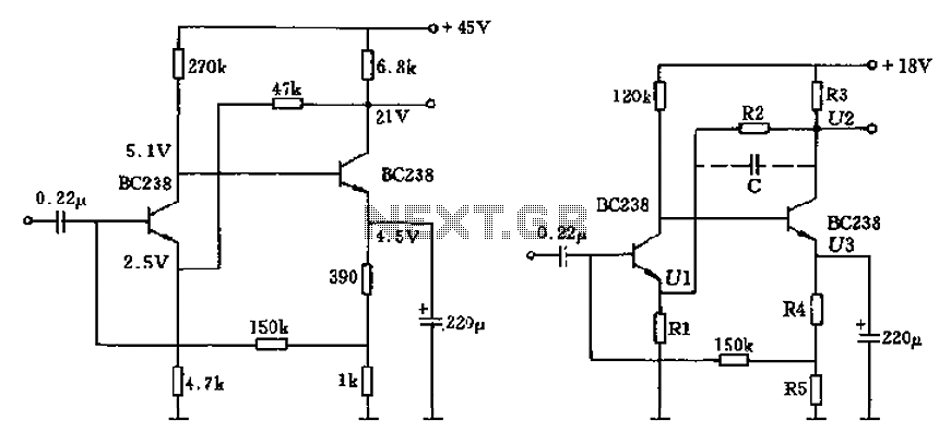
The circuit characteristic involves the elimination of external input resistors, which reduces the influence on the stabilization of the working point. It also employs two DC negative feedback loops. Additionally, the output from the second stage connects to the...
D1, D2, C1, and C2 double the AC input voltage, charging capacitor C3 through resistor R1 to approximately 320 volts. Resistor R1 isolates the voltage doubler from the discharge capacitor C3, ensuring that capacitors C1 and C2 do not...

The transistor characteristic curve tracer circuit depicted in Figure 555 illustrates the characteristics of a transistor. It utilizes two voltages: a step wave applied to the base (b) to generate different base currents (Ib), and a sawtooth waveform at...
Utilize this FM antenna amplifier in locations where the reception of FM stations is poor. This circuit is specifically designed for this purpose. The FM antenna amplifier circuit is engineered to enhance signal strength for FM radio stations, particularly in...
In linear equipment design, it is sometimes necessary to take a voltage that is referenced to a certain DC level and generate an amplified output that is also referenced. In linear circuit design, the process of amplifying a voltage that...