
RF MODULATOR

The described circuit utilizes a 7413 Schmitt-trigger oscillator configured to generate a frequency that is one-third of the target carrier frequency for a specific television channel. In this case, the oscillator is set to approximately 20 MHz, which is suitable for channel 3. The Schmitt-trigger configuration ensures a stable oscillation, providing a square wave output that can be utilized for further processing.
The buffer section of the circuit is crucial as it allows for the amplification of the square wave output, ensuring that it is robust enough to drive subsequent stages. The transistor Q1 plays a significant role in modulating the RF output. By varying the effective supply voltage to the IC, Q1 adjusts the amplitude of the RF signal, thereby controlling the modulation depth. With a standard video signal level of 1 V peak-to-peak, the design achieves a modulation depth of approximately 20% when powered by a 5-V supply. This modulation depth is sufficient for transmitting video signals effectively.
To connect the oscillator output to a television set, a capacitive coupling method is employed. This involves using short lengths of 300-ohm transmission line, which helps to minimize signal loss and reflections. The regular antenna leads are removed from the television set to facilitate this connection, allowing the modified TV set to serve as an experimental display terminal for a microprocessor, showcasing the versatility of the circuit in practical applications.
The resistor R1 is a critical component in the oscillator circuit, as it determines the frequency of oscillation. By adjusting R1, users can fine-tune the frequency to achieve the best possible reception of the desired TV channel. This feature adds flexibility to the design, making it adaptable to various conditions and requirements. Overall, the circuit exemplifies a functional approach to RF modulation and signal transmission in a television context.First section of free-running 7413 Schmitt-trigger oscillator runs at one-third of desired TV-channel carrier frequency (about 20 MHz for channel3) and drives buffer section whose output is square wave at oscillator fundamental. Q1 modulates RF output by varying effective supply voltage to IC. Since standard video is 1 V P-P, modulation depth is a bout 20% with 5-V supply. Capacitive connection is made to TV set, using short lengths of 300-ohm line after removing regular antenna leads from set used as experimental display terminal for microprocessor. R1 determines frequency of oscillation; ad just for best reception. -W, Banks, The Waterloo RF Modulator, BYTE, Jan. 1978, p94. 🔗 External reference
Related Circuits
Construct an accurate LC Meter (Capacitance Inductance Meter) to facilitate the creation of coils and inductors. This LC Meter is capable of measuring very small inductances, making it an ideal tool for various RF coil and inductor applications. The...
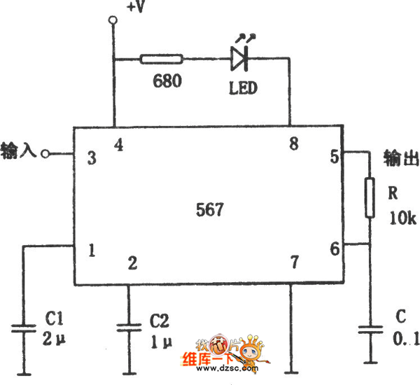
The figure illustrates the 567 FM demodulator circuit. The FM signal is received at pin 3, while the demodulated output signal is available at pin 5. The central frequency of the FM signal that the circuit can demodulate is...

This circuit is a Phase-Locked Loop (PLL) system designed for use as an FM demodulator. The output of the Voltage-Controlled Oscillator (VCO) follows the FM signal, with the input voltage to the VCO being proportional to its output frequency....
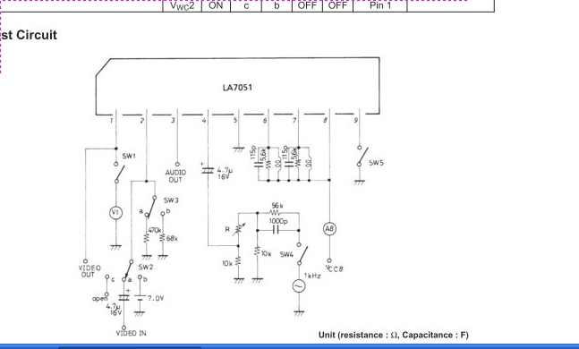
The LA7051 is a video and audio signal processor integrated circuit (IC) designed for UHF band RF modulation. It performs functions such as audio frequency modulation, video clamping, and white clipping. The LA7051 IC is engineered to facilitate the modulation...
The circuit depicted in the schematic diagram below can achieve 99% modulation with a maximum frequency of 200 kHz. The amplification of this circuit can be... This circuit is designed for high-efficiency amplitude modulation, capable of achieving a modulation depth...

The circuit is designed for satellite transmission of ECG signals with a bandwidth range of 0.5 to 50 Hz, as well as other medical data within electronic systems. An audio signal serves as the FM signal source, which is...