
PLL FM Demodulator Circuit Module

The circuit functions effectively by utilizing the CD4046B integrated circuit, which incorporates both a VCO and phase comparators. The VCO generates a frequency that is controlled by the input voltage, allowing it to lock onto the frequency of the incoming FM signal. The phase comparator compares the phase of the VCO output with the phase of the incoming FM signal to maintain synchronization.
In this setup, the AC coupling at the input stage is crucial for filtering out any DC offset present in the incoming signal, ensuring that only the varying part of the signal is processed. This is particularly important in FM demodulation, where the information is encoded in the frequency variations of the carrier wave.
The choice of Phase Comparator I is significant as it offers better performance in terms of noise rejection, which is essential in demodulating FM signals where the signal-to-noise ratio can be critical. The PLL's ability to maintain a stable output frequency that corresponds to the modulated audio signal makes it highly effective for applications in radio communications and audio processing.
Overall, this PLL-based FM demodulator circuit provides a reliable means of extracting audio information from frequency-modulated signals, making it suitable for various electronic communication systems. The design ensures that the demodulated output is a faithful reproduction of the original audio signal, which is critical for clarity and quality in audio applications.This is a circuit about PLL system that can be used to implement an FM demodulator. Since the VCO output tracks the FM signal, and the VCO input voltage is proportional to the VCO output frequency, then the VCO input will be equal to the demodulated signal. This circuit is based on phase comparator and VCO. This is the figure of the circuit. For t his example, an FM signal consisting of a 10-kHz carrier frequency was modulated by a 400-Hz audio signal. The schematic diagram shows the connections of the CD4046B as an FM demodulator. The total FM signal amplitude is 500 mV, therefore, the signal must be ac coupled to the signal input (terminal 14).
Phase comparator I is used for this application because a PLL system with a center frequency equal to the FM carrier frequency is needed. Phase comparator I lends itself to this application also because of its high signal-input-noise-rejection characteristics.
🔗 External reference
Related Circuits
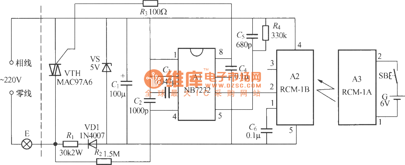
The diagram above illustrates a radio remote control dimmer circuit. This circuit utilizes a micro radio transmit/receive module in conjunction with a light modulation ASIC, resulting in a compact and easily producible design. It operates reliably and features a...
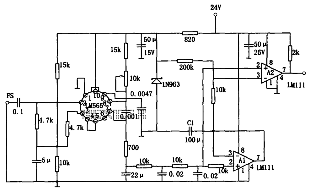
The sensitive frequency demodulation circuit utilizes the LM565 integrated circuit in a phase-locked configuration, allowing it to track frequency offsets across a wide range. However, at small frequency offsets, the signal can produce a minimal demodulated output, causing the...
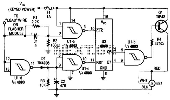
This circuit counts the flashes of turn signals. After approximately 70 flashes, a chime sounds to remind the driver to deactivate the turn signal. The period can be altered by using different taps on U2 if desired. BZ1 serves...
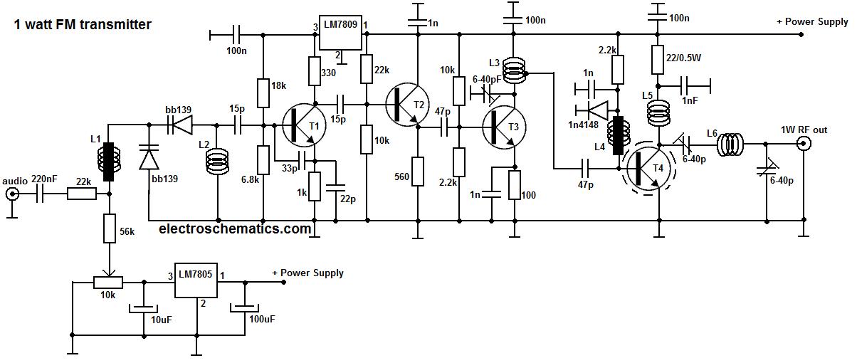
This portable FM transmitter features a limiter, a microphone amplifier, and PLL digital tuning, all integrated onto a single circuit board. The RF power output can be switched between 1 W (high) and 0.2 W (low). The schematic is...
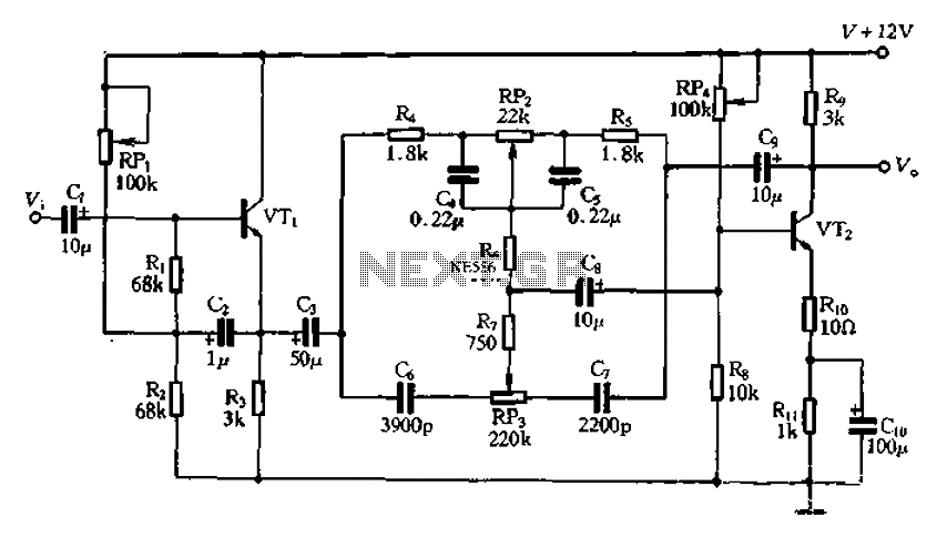
The attenuation circuit is a feedback tone control system that consists of transistors and an RC network. The circuit includes a low tone control potentiometer (RP2) and a treble control potentiometer (RP3). The bass control is influenced by resistor...

Personal Safes are revolutionary locking storage cases that open with just the touch of your finger. These products are designed as secure storage for medications, jewelry, weapons, documents, and other valuable or potentially harmful items. These utilize fingerprint recognition...
Warning: include(partials/cookie-banner.php): Failed to open stream: Permission denied in /var/www/html/nextgr/view-circuit.php on line 713
Warning: include(): Failed opening 'partials/cookie-banner.php' for inclusion (include_path='.:/usr/share/php') in /var/www/html/nextgr/view-circuit.php on line 713