
RF Module Interfacing Circuit Example

The circuit utilizes the HT12E and HT12D integrated circuits to facilitate wireless communication through an RF module. The HT12E encoder converts parallel data inputs into a serial output that can be transmitted by the RF module. The data inputs are managed through four pushbutton switches, allowing users to manually input binary values. The RF transmitter then sends the encoded data wirelessly.
On the receiving end, the RF receiver captures the transmitted signal and feeds it into the HT12D decoder, which converts the serial data back into parallel form. The decoded output is displayed through LEDs, which provide a visual representation of the received data bits. The VT pin serves as a vital indicator of the communication link status. If the link is functioning correctly, the VT LED will blink to signify successful data transmission.
For troubleshooting, it is advisable to bypass the RF components and test the encoder and decoder directly through wired connections. This step will help isolate any issues with the RF transmission or the encoder-decoder functionality. Proper attention to the connections and the integrity of the ICs is crucial for ensuring reliable operation of the circuit.I am posting here a circuit example for interfacing RF module using HT12E/D encoder decoder pair. The circuit attached here can be used to transfer data using the RF module. As I have explained earlier RF module mentioned here is having a single channel. So we can use only serial data transfers. This example uses HT12E/D encoder-decoder pair for converting the parallel data to serial and back. This encoder-decoder pair supports 4 bit parallel data. Thecircuithas two parts transmitter and receiver. In the transmitter part we are using HT12E for encoding data from parallel to serial. The serial output from the from the encoder is fed to the data IN of the RF transmitter. Four switches namely SW0, SW1, SW2, SW3 are used to input data to the decoder. These switches are pushbutton switches with active low states. (i. e. when you press it, the data input will be `0` and in the released state data input will be `1`. The default state is `1`). At the receiver section we are having RF receiver and HT12D decoder IC. The serial data from the receiver is fed into to serial input of the decoder. The parallel data is displayed with the help of LED`s. AnotherLED at the pin VT of the decoder shows whether your link is established or not. If it is ON then everything is OK. Instead if it ispermanently OFF, then there is a linkfailure. You may refer the data sheet of the IC to know the exact function of pin VT. After eachsuccessfultransmission of a 4-bit data, VT pin goes to a low state for a while and will come back to high state. Thus during the transmission you may see the LED at pin VT blinking. If your circuit is not working, just remove the RF transmitter and receiver and make a wired connection from the serial data OUT of the HT12E encoder to the serial data IN of the HT12D decoder.
Now check whether you could receive the data send from the encoder to decoder. If it is not working, you can conclude that problem is with the encoder/decoder pair. Either there will be some bugs in the circuit or your IC`smightbedamagedones. 🔗 External reference
Related Circuits
A 555 timer operating in astable mode generates driving pulses, while two 4518 dual BCD (binary coded decimal) counters provide square waves. A TL081 operational amplifier functions as an output buffer-amplifier. Potentiometers R1 and R2 are utilized to control...

The use of JFETs allows for high resistance and long time constants in this very low frequency multivibrator. The values indicated are for operation at 0.15 Hz. In the context of electronic circuit design, a multivibrator is a circuit that...

A simple metal detector electronic project circuit can be designed using the CS209A integrated circuit manufactured by Cherry Semiconductor. The CS209A integrated circuit is a bipolar monolithic integrated circuit intended for metal detection and proximity sensing applications. It incorporates...
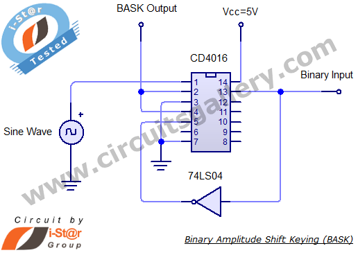
Binary Amplitude Shift Keying (BASK), also known as On-Off Keying (OOK), is a digital modulation technique where the amplitude of the carrier signal is altered according to binary data. This modulation scheme is utilized for transmitting digital information over...
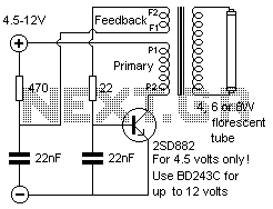
This inverter is very easy to construct, reliable, and even powerful enough to light up a 15W fluorescent tube (if you cool your transistor well). The only hard-to-find piece of this baby is the so-called yellow inverter transformer. It's...
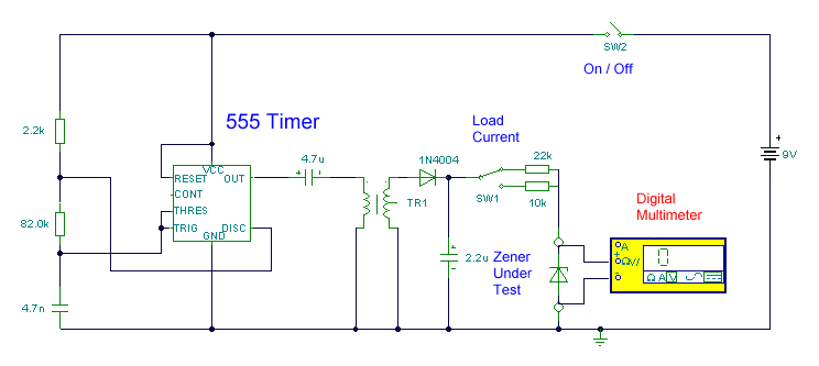
This circuit utilizes a single 555 Timer IC along with a small transformer to generate high voltage for testing zener diodes with voltage ratings up to 50VDC. The 555 timer operates in astable mode, with the output from pin...