
S1Ngle-Ic Logic Probe

The logic probe circuit is designed to diagnose and test digital circuits by indicating the logic levels present at various points in the circuit. The CD4009 hex inverter is a versatile component in this configuration, as it provides the necessary inversion of signals while maintaining a high input impedance, which is crucial for avoiding interference with the circuit under test.
The input-bias network, which consists of resistors R1 and R3, is critical for establishing the default state of the inverters. When the circuit is not connected to any logic level, the biasing ensures that both outputs remain low, preventing false indications. This is particularly important in scenarios where the probe may be inadvertently left floating, as it helps avoid misleading readings.
When the probe is applied to a logic low, the circuit behavior changes. The low input causes inverter 3 to output a high signal, which in turn influences the states of inverters 1 and 2. This cascading effect is a fundamental aspect of the logic probe's operation, enabling it to clearly indicate the presence of a low logic level by illuminating LED 1.
The two LEDs serve as visual indicators of the logic states. LED 1 indicates a logic high output from inverters 1 and 2, while LED 2 indicates the state of inverters 4 and 5. The careful arrangement of resistors and inverters allows for a straightforward and effective means of monitoring digital signals, making this logic probe a valuable tool for electronics testing and troubleshooting.
Overall, this logic probe circuit exemplifies a practical application of CMOS technology in digital electronics, providing an efficient and reliable method for assessing logic levels in various electronic systems. This logic probe uses a CD4009 CMOS hex inverter. The characteristic high-input impedance of CMOS gives the advantage of not loading the circuit being tested. Because the output of the inverters is not specified at either a high or low level with a floating input, an input-bias network produces lows at both input inverter pairs if the input is open or at less than 2 V. Resistor R3 holds the input of inverter 3 low which makes the output of inverters 4 and 5 low and will not permit LED 2 to light.
At the same time, Rl holds the inputs of inverters 1 and 2 high so that their output is low and LED 1 will not light. If the probe input is touched to a logic low, the output of inverter 3 is held high by R3 and inverter 1 and 2 are brought low, which causes their outputs to go high and turns on LED 1.
With no input, both LEDs should be off.
Related Circuits
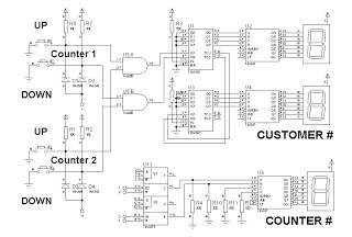
This is a simplified design utilizing an up/down counter integrated circuit (IC), specifically the 74192. This versatile logic IC features separate pins for counting both up and down. Additionally, an RS latch is incorporated to indicate the current counter...
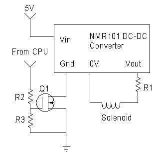
Despite exhaustive searching, every reasonably priced solenoid valve for controlling propane during pushbutton start required 12VDC, beyond the capabilities of a normal pump battery. There are methods to generate HV pulses which will actuate the solenoid, which will remain...
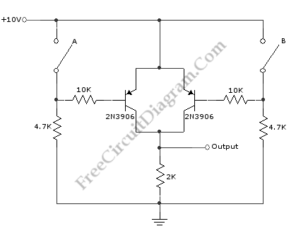
This schematic diagram illustrates a basic logic gate circuit. This PNP transistor circuit can function as either an OR gate or an AND gate, depending on the input states. The described circuit employs PNP transistors to create a versatile logic...
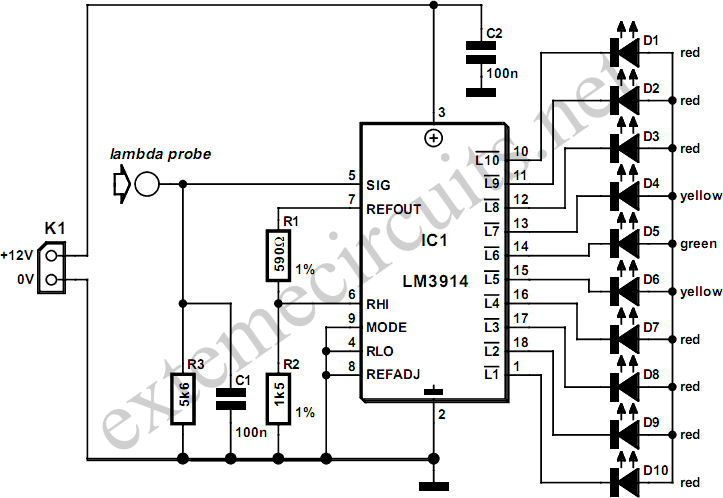
A lambda probe, also known as an oxygen sensor, is typically located on the exhaust system of most vehicles that operate on unleaded fuel. It functions effectively once it has reached its normal operating temperature. A lambda probe is a...
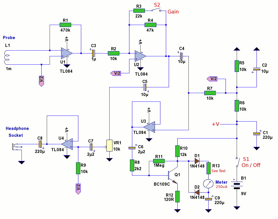
An electromagnetic field probe designed to detect changing electric and magnetic fields. The probe features switchable gain, a frequency response of up to 400 kHz, and independent audio and meter monitoring. This EMF probe utilizes an inductor to locate...
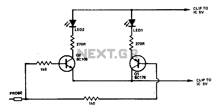
If the probe is connected to logic 0, Q1 will be activated, illuminating D1. When connected to logic 1, Q2 will be activated, illuminating D2. Any NPN or PNP transistors can be used for Q1 and Q2. Likewise, D1...