
Basic Logic Gate with PNP Transistor
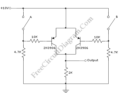
The described circuit employs PNP transistors to create a versatile logic gate configuration. In digital electronics, logic gates are fundamental building blocks used to perform logical operations on one or more binary inputs to produce a single binary output.
In this specific schematic, the PNP transistor can be configured to operate as an OR gate when the inputs are connected in such a way that if either input is activated (i.e., brought to a low state), the output will also be activated (high state). Conversely, when configured as an AND gate, the circuit will only output a high state when both inputs are in a low state.
The operation of the PNP transistor is based on the principle that it conducts when the base is at a lower potential than the emitter. Therefore, the arrangement of resistors and the connections to the inputs are critical to achieving the desired logical functionality.
The transistor's biasing must be carefully considered to ensure that the desired logic levels are correctly interpreted. Resistors may be used to limit the current flowing into the base of the transistor and to establish the necessary voltage levels for proper operation.
In practical applications, this circuit can be utilized in various digital systems, including simple calculators, alarm systems, and other devices requiring basic logical decision-making capabilities. The simplicity of the PNP transistor circuit allows for easy integration into larger systems while providing reliable performance.
Overall, this schematic serves as a foundational example of how PNP transistors can be employed in digital logic design, showcasing their versatility and importance in electronic circuit design.This schematic diagram shows a circuit of basic logic gate circuit. This PNP transistor circuit can act as OR gate or AND gate. If the input is closing of. 🔗 External reference
Related Circuits
The AN6657 is a 16-pin dual in-line plastic package, while the AN6657S features a 16-pin dual flat plastic package. The speed control function operates with an internal H-bridge driver chip circuit, utilizing pins 5 and 8 for H-bridge driver...
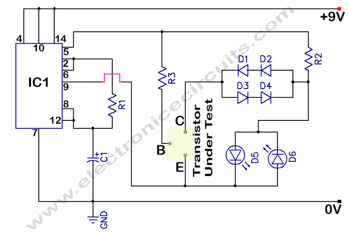
The circuit is a transistor tester schematic that indicates the condition of a transistor using two LEDs. It is designed to test a good NPN transistor. The transistor tester circuit operates by utilizing two light-emitting diodes (LEDs) to provide a...
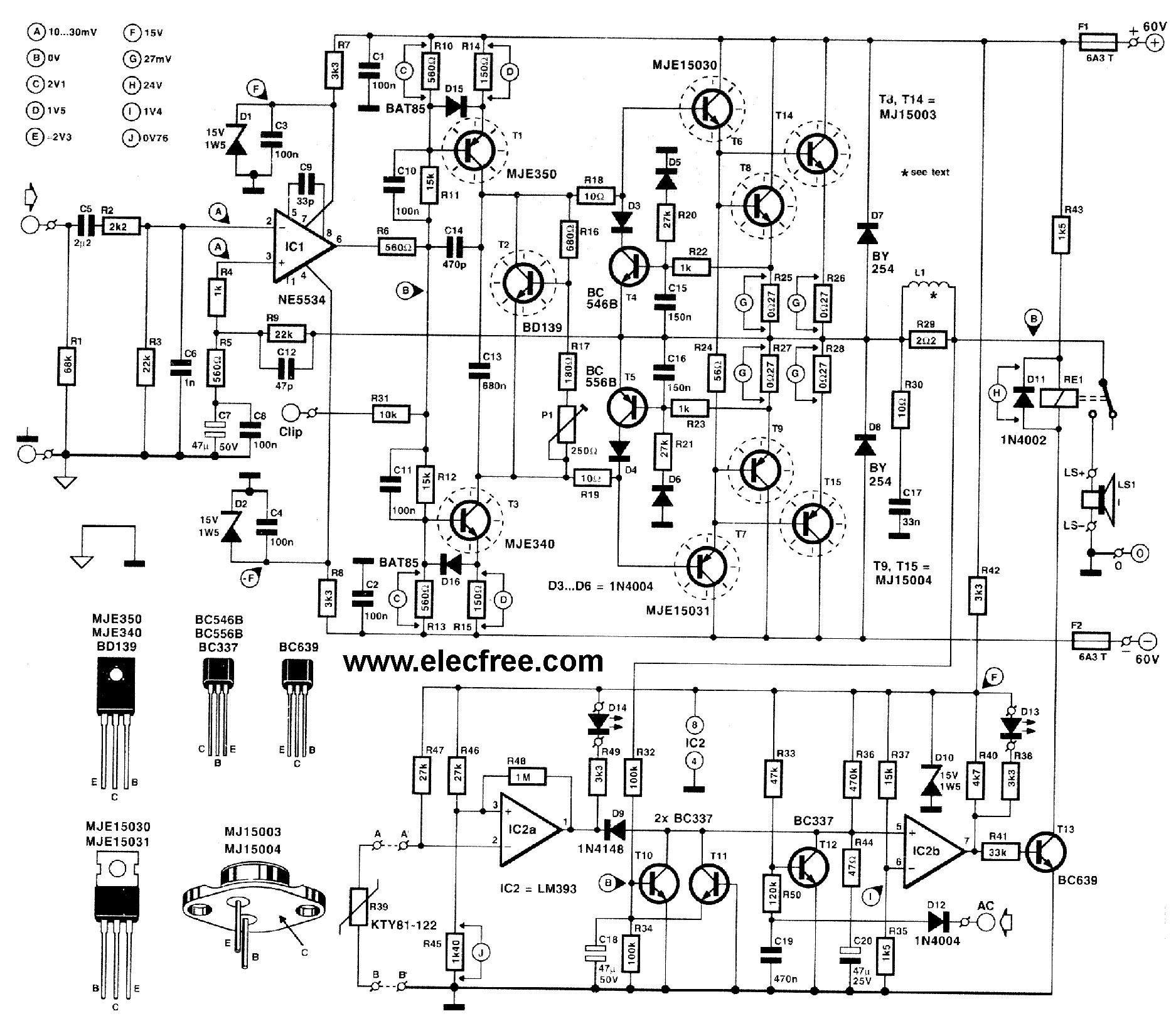
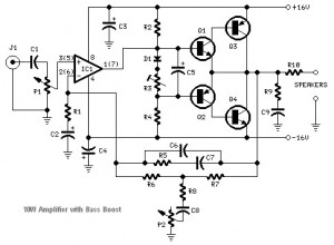
This circuit is designed for friends who are interested in high-power amplifier circuits. It can deliver approximately 300 Watts RMS and operates as an OCL (Output Capacitor-Less) Class AB amplifier, providing high sound power while systematically protecting the loudspeaker...
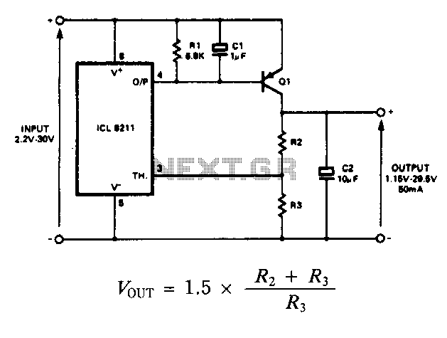
The IC8211 serves as the voltage reference and regulator amplifier, with Q1 functioning as the series pass transistor. Resistor R1 defines the output current of the IC8211, while capacitors C1 and C2 ensure loop stability and help suppress the...
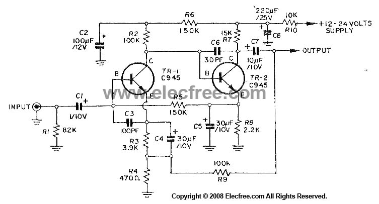
This circuit utilizes three transistors (2SC945, 2C1815, or 2SC828) as the primary components, functioning as a typical low-noise transistor amplifier. It offers a gain of approximately 200 to 300 times and has a frequency response ranging from 50Hz to...
This audio amplifier circuit is based on the operational amplifier NE5532 and utilizes a pair of power transistors, TIP41A and TIP42A. It is capable of delivering up to 10W of audio power output into an 8-ohm speaker. The design...