
Safe Sync to Adapt Digital Camera to Higher Voltage Flash
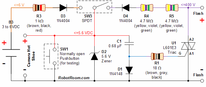
This circuit is designed to provide a reliable interface between a camera and a flash unit, ensuring proper operation while safeguarding sensitive components from potential damage. The triac serves as the primary switching element, allowing for controlled discharge of the flash capacitor while maintaining safety features such as reversed polarity protection through the use of diodes. The inclusion of resistors in the design not only manages current flow but also facilitates the necessary voltage drop to prevent damage to the Zener diode and the camera itself. The choice of components, including the specific triac and diodes, reflects a careful consideration of the operational requirements and safety parameters, ensuring that the circuit functions effectively within its specified limits. Overall, this circuit exemplifies a well-thought-out design that balances performance and protection for photographic applications involving flash photography.This circuit adds a datasheet-compliant trigger signal, reversed polarity protection, optional test button, and optional battery operation. U1 L601E3 or MAC97A8 triac. 400 V, 1 A. When U1 is enabled, the + and - wires of the flash are electrically connected, just as though the camera hot shoe had done so.
A triac is a semiconductor switch, similar to a bipolar or MOSFET transistor, except that it won`t conduct in either direction unless turned on at the gate, and it won`t turn off until the current across it subsides. This is beneficial for a flash, since it allows the high voltage to fully dissipate, even if the camera doesn`t assert the trigger signal long enough.
R1 18 © resistor. This limits the current passing through the gate of U1; to keep the current below 1 amp and to extend the amount of time it remains triggered in order to meet the 2. 5 µs minimum. Both of these limits are specified by the L601E3 datasheet. Furthermore, this limits the amount of current across the camera hot shoe during discharge. D1 1N4148 or 1N914 diode. This is a one-way path that allows capacitor C1 to charge, but won`t allow it to discharge except through the gate of the triac.
(Pictures of the current flow are presented on the next page. ) The type of diode selected has a relatively low voltage drop, in comparison to the 1N4004 diodes, to allow C1 to charge almost completely. D2 5. 6 V Zener diode. This protects the camera by limiting the maximum voltage across the camera shoe to no more than 5. 6 V. A higher-voltage Zener diode runs the risk of damage to the camera. A lower-voltage Zener diode reduces the maximum charge voltage of capacitor C1, which may prevent triac U1 from triggering.
R4 and R5 Two 4. 7 M © resistors. These limit the amount of current that can flow from the flash, reducing voltage along the way. If too much current flows, the Zener diode can be damaged, it wastes power, and the flash may either constantly trigger or never trigger. Multiple resistors are used in series instead of a single resistor, since there is a limit on how much voltage a single resistor can handle across it.
If you are not going to connect up to a 400 V flash, you can reduce the resistance to speed cycle time (reduce the time it takes to charge the circuit from the flash). D3 and D4 Two 1N4004 diodes. These diodes are one-way paths. If the selected power source is connected backwards (reverse polarity, + and - swapped), it won`t harm the camera with a negative voltage across the hot shoe, because the diode
🔗 External reference
Related Circuits
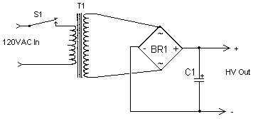
The circuit can produce about 250-500mA at 2KV, depending on the transformer. For C1, you can use the capacitor out of an old microwave. This circuit is mainly provided as a demonstration of using commonly available parts for something...
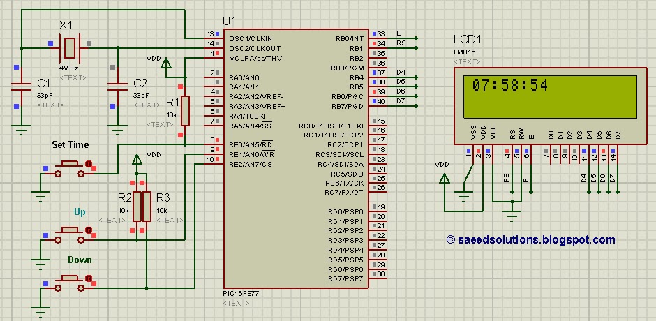
This tutorial on the PIC16F877 microcontroller addresses the question, "How to implement a controllable digital clock using the PIC16F877?" It utilizes the PIC16 simulator for demonstration purposes. The implementation of a controllable digital clock using the PIC16F877 microcontroller involves several...
The LinkSwitch-XT LNK363DN-based flyback power supply generates a single isolated DC output voltage from an input voltage range of 90 VAC to 264 VAC. The power supply delivers an output of 5 V at 550 mA (2.75 W) in...
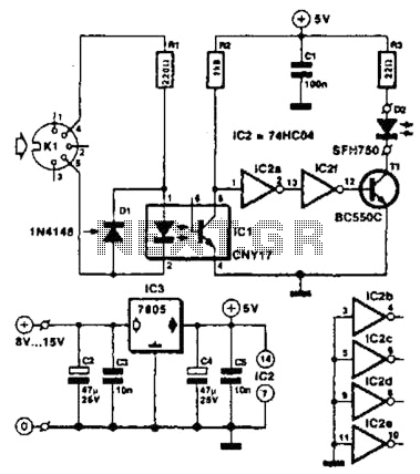
Used for digital control of musical instruments, this transmitter converts digital data signals into equivalent optical signals for a fiber optic cable interface. Optocoupler IC1 provides isolation, driving IC2-a and -b, and T1, ultimately providing a cable driver LED...

This circuit measures the distance covered during a walk. The hardware is housed in a small box that can be slipped into a pocket. The display is arranged such that the leftmost display, D2 (the most significant digit), shows...
In the precision circuit, an operational amplifier provides a buffered output and also functions as a 2-pole filter. The ripple will be less than 5 mV peak for all frequencies above 1 kHz, and the response time will be...
Warning: include(partials/cookie-banner.php): Failed to open stream: Permission denied in /var/www/html/nextgr/view-circuit.php on line 713
Warning: include(): Failed opening 'partials/cookie-banner.php' for inclusion (include_path='.:/usr/share/php') in /var/www/html/nextgr/view-circuit.php on line 713