
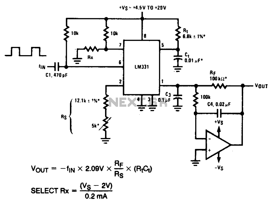
Precision frequency-to-voltage converter
Inherently, the voltage-to-frequency (V-to-F) converter response can be fast, while the frequency-to-voltage (F-to-V) response is limited.
The operational amplifier (op-amp) in this precision circuit serves multiple functions, including buffering the output signal to isolate the circuit stages and minimizing signal degradation. The 2-pole filter configuration is designed to attenuate unwanted high-frequency noise while maintaining an acceptable signal integrity within the desired frequency range. The filter's cutoff frequency is set to allow signals above 1 kHz to pass with minimal ripple, quantified as less than 5 mV peak. This specification is crucial for applications requiring high precision and low distortion.
The filter's performance is influenced by its time constants, which are determined by the resistive and capacitive components in the circuit. The engineering challenge lies in selecting these components to balance the speed of response with the ripple characteristics. A thorough analysis of the filter's behavior at lower frequencies reveals that the ripple increases for input signals below 200 Hz, indicating that the filter may not be suitable for all applications without further modifications.
Furthermore, the inherent differences between V-to-F and F-to-V conversion processes are noteworthy. The V-to-F converter can achieve rapid response times due to the nature of the conversion, which is typically faster than the reverse process. In contrast, the F-to-V converter may introduce additional latency, which could affect overall system performance in applications requiring fast and accurate signal processing.
Overall, the design of this precision circuit requires careful consideration of the operational amplifier's characteristics, filter configurations, and the specific application requirements to ensure optimal performance across the intended frequency range.In the precision circuit, an operational amplifier provides a buffered output and also acts as a 2-pole filter. The ripple will beless than 5 mV peak for all frequencies above 1 kHz, and the response time will be much quicker than in Part 1.
However, for input frequencies below 200 Hz, this circuit will have worse ripple than the figure. The engineering of the filter time-constants to get adequate response and small enough ripple simply requires a study of the compromises to be made. Inherently, V-to-F converter response can be fast, but F-to-V response cannot. 🔗 External reference
Related Circuits
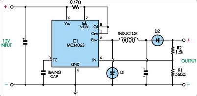
This circuit utilizes mobile phone chargers that incorporate the Motorola MC34063 switch-mode integrated circuit (IC). The output voltage can be adjusted across a broad spectrum by altering the values of the feedback resistors R1 and R2. The output voltage...
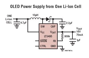
The LT3495, LT3495B, LT3495-1, and LT3495B-1 are low-noise boost converters equipped with an integrated power switch, feedback resistor, and output disconnect circuitry. These devices manage power delivery by adjusting both the peak inductor current and the switch off-time, resulting...
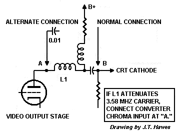
The D 101-2 depends on the television to supply a wide bandwidth video signal. Most black-and-white TVs from 1954 onward contain narrowband intermediate frequency (IF) strips or low-pass filters. A wide passband is a disadvantage because it picks up...
The lack of compensation facilitates the processes of development and testing. The figure of 6 billion frequently appears as the estimated number of cell phones in use globally. Published estimates indicate an average. The discussion of compensation in electronic circuits...
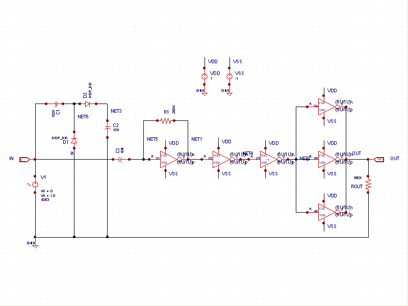
This schematic example demonstrates a sinusoidal voltage input at a frequency of 10 kHz, which is converted to a square wave using an inverter-based circuit. The VDD and VSS rails are connected to +1V and -1V, respectively. The control...
It has been mentioned that the operational amplifier (op amp) in the second stage may be damaged. Confirmation is requested by testing the op amp in a buffer configuration or any simple configuration. This test is necessary to ascertain...