
Schematic circuit diagram of low voltage and low voltage automatic conversion
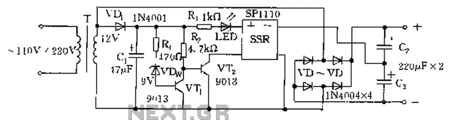
The circuit design involves several key components that work together to convert high voltage AC to a stable low voltage DC output suitable for powering LEDs or other low-voltage devices. The transformer T is essential for stepping down the initial 220V AC supply, which is then processed by the diodes in the bridge rectifier configuration. This arrangement ensures that the AC input is converted to a pulsating DC output. The role of capacitors C2 and C3 is critical, as they smooth out the rectified output, reducing ripple and providing a more stable DC voltage level.
In the event of a reduced input voltage of 110V AC, the circuit adapts by utilizing the remaining components effectively. Transistor VT2 continues to conduct, allowing the SSR to activate and maintain the output voltage through the voltage doubler configuration formed with diodes VD2 and VD3. This clever arrangement allows the circuit to maintain functionality even under lower input voltage conditions, ensuring that the LED remains illuminated.
Overall, the circuit exemplifies a robust design that can efficiently manage voltage conversion and regulation, making it suitable for various low-voltage applications while ensuring reliability across different input voltage scenarios. Below is automatically converted to low-voltage circuit. 220V electricity through step-down transformer T after, VDw breakdown camel guide so VT1, VT2 off, solid state relays S SR is turned off, this time by VD2 ~ VD5 bridge rectifier, C3 C2 filtered stream output DC voltage of approximately 14V; when when the AC input voltage is 110V, by T buck insufficient wear VDw, VT1 off, VT2 conduction, SSR is turned on. In this case, SSR, VD2 ~ VD3 and C2, C3 composed of a voltage doubler circuit, the output DC voltage of about 14V is still.
And LED lights.
Related Circuits
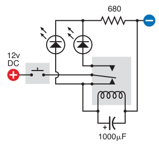
The intended result is for the relay to oscillate and the LEDs to flash when the button is pressed. However, when the button is pressed, the leftmost LED lights constantly, and nothing else happens. There is voltage across the...
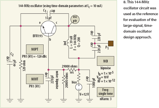
Unlike conventional small-signal methods, employing large-signal, time-domain design techniques facilitates the creation of low-noise grounded-base oscillators suitable for VHF/UHF applications. The development of low-noise grounded-base oscillators for VHF/UHF applications presents unique challenges and opportunities. By utilizing large-signal, time-domain design techniques,...
In pulse position modulation, the amplitude and width of the pulses are kept constant, while the position of each pulse with reference to the position of the reference pulse is changed according to the instantaneous sampled value of the...
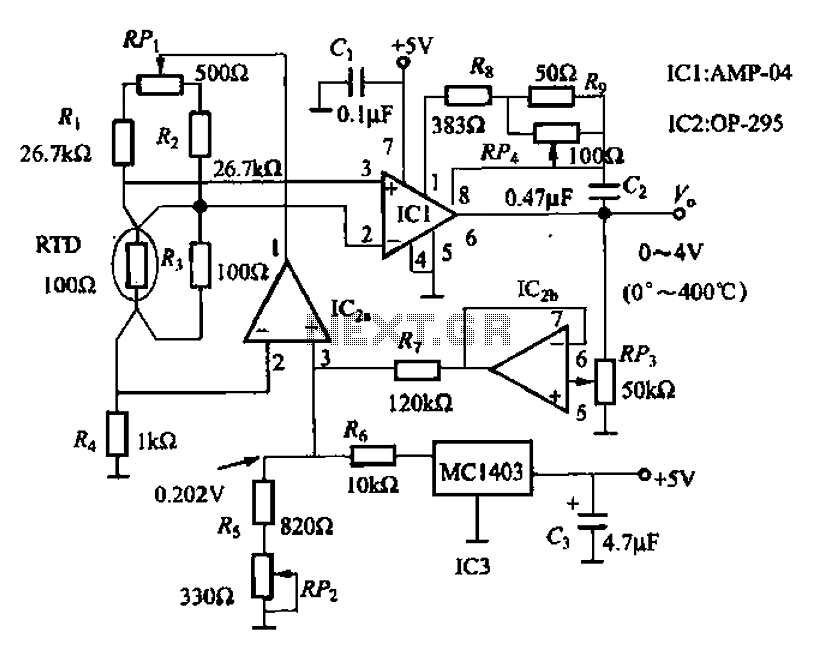
AMP-04 is a single-supply, single resistor gain adjustment circuit with an input voltage drift of less than 150 pV, a current drift of 5 nA, and a temperature drift of 8 pA/°C. The gain nonlinearity is 0.005% of the...
This 49-MHz FM transmitter comprises an audio amplifier, a low-pass filter, three RF stages, and a regulated DC power supply. The output power is approximately 16 mW into a 50-ohm load. This transmitter is suitable for various 49-MHz applications,...
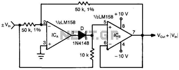
When the input voltage is positive, the output of ICA is negative, resulting in diode D not conducting; therefore, the output of ICB is positive. Conversely, when the input is negative, the output of ICA becomes positive. Diode D...
Warning: include(partials/cookie-banner.php): Failed to open stream: Permission denied in /var/www/html/nextgr/view-circuit.php on line 713
Warning: include(): Failed opening 'partials/cookie-banner.php' for inclusion (include_path='.:/usr/share/php') in /var/www/html/nextgr/view-circuit.php on line 713