
AMP-04 0 F 400 temperature measurement circuit

AMP-04 is an advanced temperature measurement circuit utilizing a high-resolution operational amplifier to achieve precise temperature readings. The circuit is designed to operate with a single power supply, simplifying the overall design and reducing power consumption. The input voltage drift of less than 150 pV ensures that the measurement remains accurate over varying conditions, while the low current drift of 5 nA and temperature drift of 8 pA/°C contribute to the stability and reliability of the circuit.
The temperature detection mechanism is based on a bridge circuit formed by resistors R1, R2, R3, and the RTD. This configuration allows for high sensitivity to temperature changes. The adjustment resistor RP plays a crucial role in balancing the bridge, which is essential for accurate measurements. The constant current sources IC2 and IC3 are vital for ensuring that the bridge operates under stable conditions, with IC3 providing a precise reference voltage of 2.500V, which is critical for the linearity and accuracy of the output.
The gain adjustment feature is implemented through the use of external resistors connected to the output pin of IC1, enabling fine-tuning of the output voltage. The trimmer resistor RP4 allows for adjustments to the gain, accommodating variations in the system or environmental factors. The output voltage range of 0 to 4.0V corresponding to the temperature range of 0 to 400°C provides a clear and interpretable signal for further processing or display.
The calibration process described ensures that the circuit is accurately set up for real-world temperature measurements. By substituting known resistances for the RTD during debugging, the circuit can be adjusted to achieve the desired output voltages at specified temperatures, confirming the accuracy of the temperature readings. This systematic approach to calibration enhances the reliability of the AMP-04 circuit in practical applications.AMP - 04 is a single-supply, single resistor gain adjustment, the input voltage drift of less than 150 pLV, the current drift in 5nA, temperature drift of 8 pA/aC, gain nonline arity of 0.005% of the high resolution op-amp. AMP - 04 0.400qC temperature measurement circuit shown in Figure 1-13. Temperature range of the circuit is 0-4000C, measurement accuracy of 0.5. Ri - R3, RPi, RTD constitute a bridge temperature detection circuit, RP, adjust the bridge balance; IC2, IC3 as a constant current source, 1C3 output 2. 500V precision reference voltage, the Rs, R6, RP2 regulation, the IC2. (+) Terminal potential is 0. 202V, IC2. Constant output current is applied across the bridge. Temperature bridge output directly to Icl amplified, O pin external resistor adjusts gain benefits, RP4 trim gain.
At a temperature of 0 to 4000C when changes, the output voltage of O-4. OV. When debugging, first with a 100. 00Q electrical resistance (equivalent to 0 ) instead of the RTD, transfer RPi, so that the output voltage is 0.oOv; then respectively 247.04 (equivalent to 400C), 175 84n resistance (fairly. at 200C) in place of RTD, respectively adjust RP4, RP3 output voltages are 4.00,2.OOV.
Related Circuits
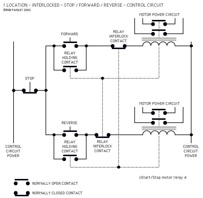
The circuits on this page are for motor controls using Push buttons and would typically be found in commercial and industrial installations. The circuits do not show the wiring of the motors themselves as this depends on the particular...
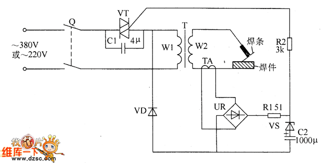
The welder no-load power saver circuit consists of a current detection control circuit and a power saving control circuit, as illustrated in the accompanying chart. The current detection control circuit includes a current transformer (TA), a bridge rectifier (UR),...

The circuit depicted in Figure 3-190 includes an armature circuit with two startup resistors, Ri and Rz, connected in series through the main switch SA to facilitate starting, stopping, and speed control. During the startup phase, two relays, KTi...
Children often go missing, causing immense suffering and economic losses for families. This situation also presents opportunities for unscrupulous child traffickers to exploit. To address this issue, a radio alarm system has been designed, which consists of a transmitter...

This is a luminous flux test circuit that utilizes optical resistors. In the circuit, the optical resistor RG forms a bridge with resistors RP1, RP2, R1, and R2. RP1 is employed to balance the bridge, while RP2 is used...

The inverter circuit diagram utilizing the NE555 timer is illustrated, designed to convert a +12V DC battery voltage into a 220V AC output voltage. In this circuit, the NE555 functions as an oscillator, with the oscillation frequency determined by...
Warning: include(partials/cookie-banner.php): Failed to open stream: Permission denied in /var/www/html/nextgr/view-circuit.php on line 713
Warning: include(): Failed opening 'partials/cookie-banner.php' for inclusion (include_path='.:/usr/share/php') in /var/www/html/nextgr/view-circuit.php on line 713