
Schematic Diagram 100W 2x LM3886 Audio Power Amplifier

The PCB layout is designed to separate the power ground from the signal ground, with the signal ground located centrally and surrounded by the power ground, connected by a thin trace near C5. The PCB layout was created using PADS PowerPCB 5.0, which is considered powerful layout software. A regulated power supply is employed, featuring 10,000µF per rail before the LT1083 regulator, and 100µF on the regulator board. The use of regulation effectively removes power supply ripple voltage, which would otherwise introduce audible 50/100Hz hum from the speaker. A high-current MUR860 diode is utilized to ensure sufficient current flow, while the LT1083 voltage regulator can provide approximately 8A of current. The transformer used is a 500VA unit with dual 25V outputs, resulting in a regulated output voltage of 30V after passing through two LT1083 regulators. DC measurements indicate a low 7mV DC offset at the speaker terminals, with a voltage difference of less than 1mV between the outputs of the two chips. The sound quality of this amplifier is reported to be similar to that of an LM3875 amplifier, characterized by clarity and detail, with no hum, hiss, or noise. Compared to the LM3875 Gainclone, this amplifier delivers twice the power to a 4-ohm speaker, significantly improving dynamics and bass response.
The design of this audio amplifier highlights several important features that contribute to its performance. The parallel configuration of the LM3886 chips allows for increased power output while maintaining sound fidelity. The choice of high-quality capacitors ensures that the amplifier can handle audio signals without introducing unwanted artifacts. The separation of power and signal grounds in the PCB layout minimizes interference, which is crucial for high-fidelity audio applications. Furthermore, the regulated power supply design helps to maintain voltage stability under varying load conditions, which is essential for consistent audio performance. The careful selection of components, combined with a thoughtful PCB layout, results in an amplifier capable of delivering clean, powerful audio suitable for demanding listening environments.This audio amplifier designed uses two LM3886 per channel, in parallel circuit, based on the PA100 parallel amplifier detailed in National Semiconductor`s application note - AN1192. This amplifier can deliver about 50W into a 8-ohm speaker and 100W into a 4-ohm speaker. This is a stereo amplifier and therefore 4 LM3886s are used. The LM3886 circuit is in a non-inverted configuration, so the input impedance is determined by the input resistor R1, i. e. 47k. The 680 ohm and 470pF resistor capacitor filter network is used to filter out the high frequency noise at the RCA input.
The 220pF C4 and C8 capacitors are used to shot out the high frequency noise at the LM3886 input pins. I used high quality audio grade capacitors at several locations: 1uF Auricap at the input for DC blocking, 100uF Blackgate for C2 and C6, and 1000uF Blackgate at the supply filter.
The PCB is designed in a way that the power ground is separated from the signal ground, as you can see from the below layout. The signal ground is located in the middle and surrounded by the power ground. There is a thin trace near C5 connecting them. The PCB layout is done by using PADS PowerPCB 5. 0. I think it is a powerful layout software. The power supply used is a regulated power supply. I used 10000uF per rail before the LT1083 regulator. After the regulator, I have 100uF on the regulator board. The advantage of using regulator is that the power supply ripple voltage is removed. If power regulation is not used, I can hear very little 50/100Hz hum from the speaker. The high current MUR860 diode is used to ensure high current flow. The voltage regulator used is LT1083, it can provide about 8A of current. Transformer used here is a 500VA 2x 25V. The power supply is then regulated by 2 LT1083, after the regulation, the voltage is 30V. I did some DC measurement and the result is quite good, I got 7 mV of DC offset at the speaker terminal.
The voltage difference between the output of the 2 chips is less then 1 mV. The sound of this amplifier is similar to my LM3875 amplifier, which is very clean and detail. It has no hum, no hiss and no noise. Compared to the LM3875 Gainclone, this amp can deliver twice the power to my 4-ohm speaker, and it improves the dynamics and bass punch a lot. 🔗 External reference
Related Circuits
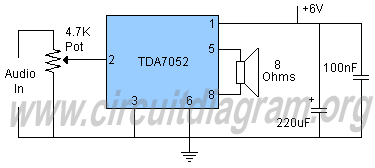
Schematic diagram and description of a 2-watt audio amplifier circuit using the TDA7052 amplifier IC. This is a very simple audio amplifier circuit. The 2-watt audio amplifier circuit utilizing the TDA7052 integrated circuit (IC) is designed for basic audio amplification...
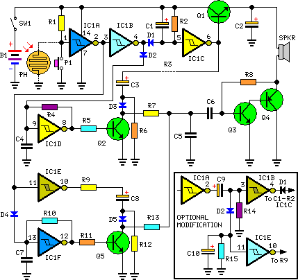
This circuit generates dual-tone bell ringing similar to most doorbell units. It can be used in various applications beyond just doorbells. Several options will be provided in the notes to accommodate different needs. The circuit, as depicted in the...
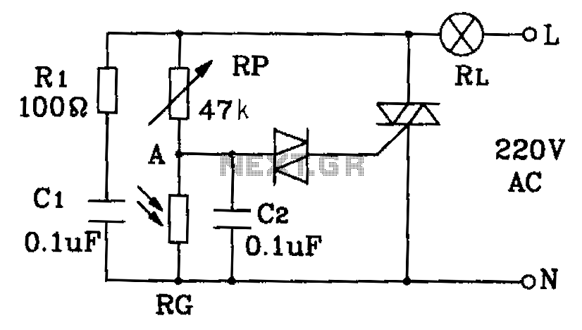
This circuit diagram illustrates an automatic lighting system designed for use in hospitals, dormitories, corridors, and public spaces. The system utilizes a photosensitive resistor to control the lighting, ensuring that lights are automatically turned off during the day and...
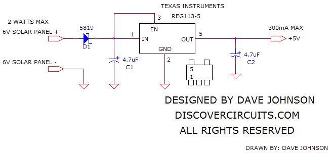
The simple circuit below regulates the voltage from a 6V solar panel to a fixed +5V. This voltage can be supplied to any cell phone or USB-connected portable device to charge its battery. The circuit utilizes a Reg113-5 voltage...
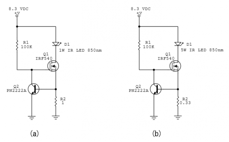
A constant-current power LED driver circuit is depicted in the schematic. Q1 is activated by R1 and functions as a variable resistor. Q2 serves as an “over-current” switch, while R2 establishes the maximum current. For the power LEDs utilized,...
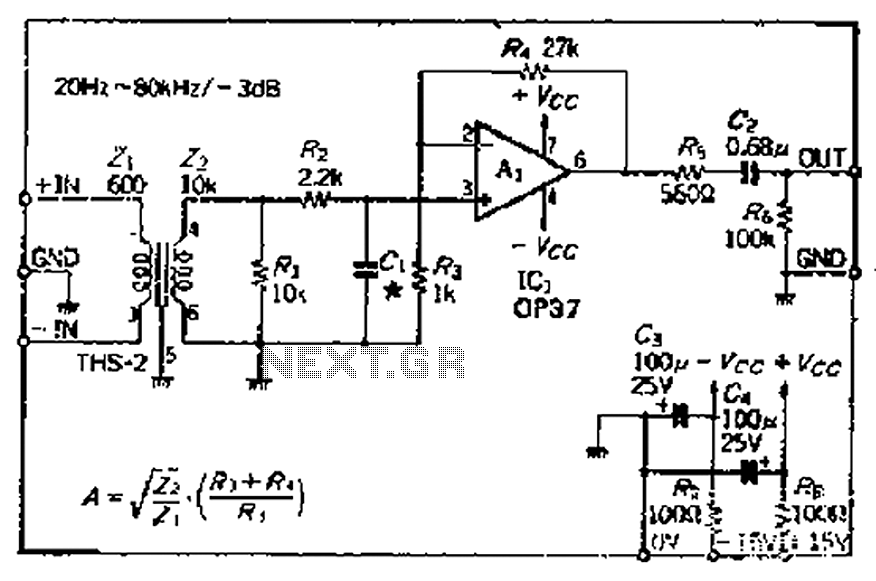
The common mode signal rejection ratio is influenced by the input transformer, which should either be a commercially available or a well-balanced homemade transformer. It is important to note that as frequency increases, the balance may decrease. The transmission...