
SCR UJI TIME DELAY
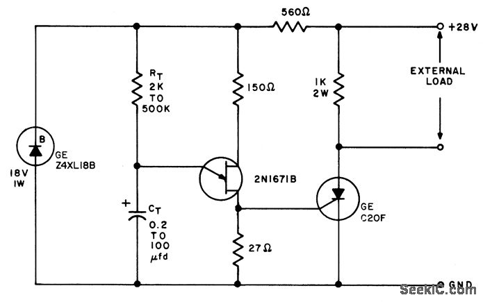
The described circuit utilizes a timing mechanism that relies on the charging and discharging characteristics of an RC network, specifically configured with a resistor (RT) and capacitor (CT). When power is applied, the capacitor begins to charge through the resistor, and the time it takes to reach a certain voltage threshold determines the timing interval. This threshold is crucial for the operation of the unijunction transistor (UJT), which serves as a triggering device.
Once the capacitor voltage reaches the UJT's firing point, the UJT conducts, allowing current to flow and triggering the silicon controlled rectifier (SCR). The SCR then turns on, providing a path for current to flow to the load, effectively applying the supply voltage. The load can vary widely, depending on the application, and may include anything from a simple LED to more complex devices.
The delay range of 0.4 milliseconds to 1 minute offers flexibility for various applications, making this circuit suitable for timing tasks in industrial automation, lighting control, or other electronic systems requiring precise timing operations. The ability to adjust the resistor and capacitor values allows for fine-tuning of the timing interval, accommodating different operational needs.
In summary, this circuit exemplifies a straightforward yet effective method for generating timed outputs using basic electronic components, demonstrating the principles of RC timing circuits and the functionality of unijunction transistors and silicon controlled rectifiers in practical applications.Timing interval is initiated by applying power, and is determined by RT-CT. At end of interval, unijunction transistor triggers silicon controlled rectifier, to apply essentially full supply voltage to load. Delay range is from 0. 4millisec to 1 minute. -"Transistor Manual, " Seventh Edition, General Electric Co. 1964, p 321. 🔗 External reference
Related Circuits
The UTC CXA1191 is a one-chip AM/FM radio integrated circuit (IC) designed for use in radio-cassette tape recorders and headphone tape recorders. It is produced by LianShun Electronics Co., Ltd. The UTC CXA1191 is engineered to provide a compact solution...
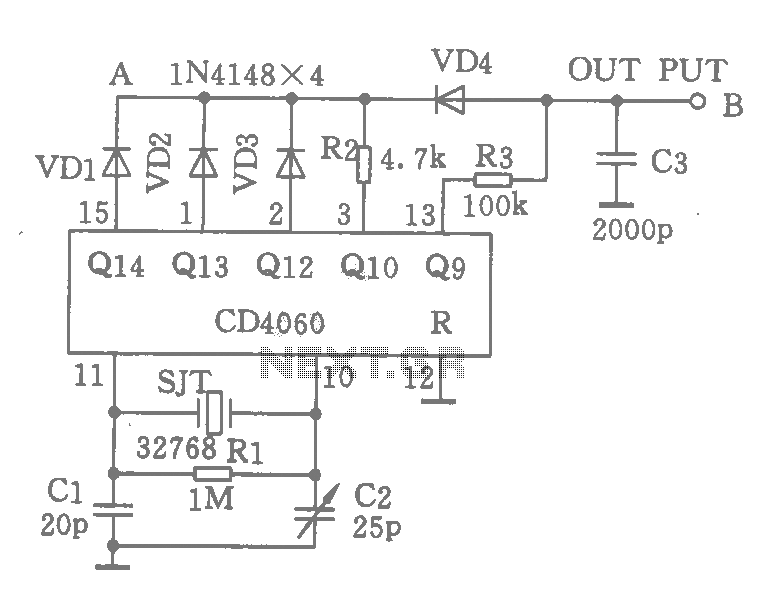
A CD4060 integrated circuit, combined with a 32,768 Hz crystal oscillator, is utilized to create a highly accurate clock source that generates 60 pulses per second. The operation is based on the division of the 32,768 Hz pulse output...
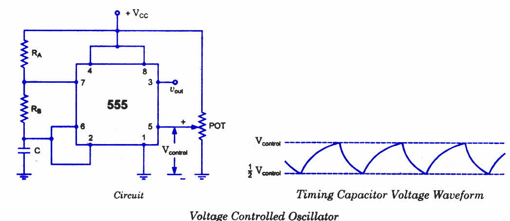
As discussed in previous blog posts, the pin 5 terminal serves as a voltage control terminal, allowing for the adjustment of threshold and trigger levels. Typically, the control voltage is set at +2/3VCC due to the internal voltage divider....
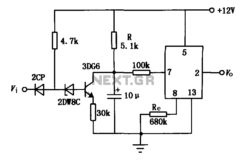
The delay application circuit is depicted in Figure JEC-2, which consists of two components. When the input transitions from logic level 0 to 1, the output also changes to 1 immediately. However, when the input transitions from high level...
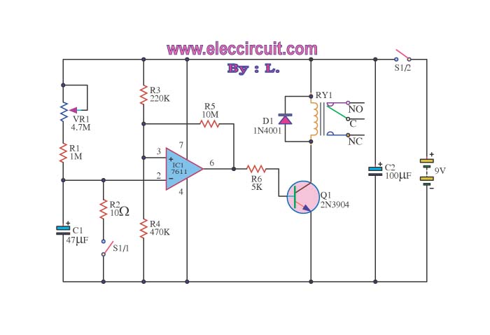
When switch S1/2 is activated, it powers the circuit C1, which utilizes the UA741 operational amplifier for voltage comparison. Pin 3 serves as the non-inverting input, while pin 2 is the inverting input. The voltage at pin 3 is...
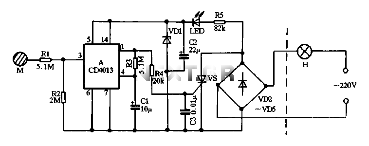
Diodes VD2 to VD5 and SCR form the main circuit of a touch switch. Resistor R5 and diode VD1 create a power supply circuit that outputs approximately 12V DC, which is utilized for a manifold A application. The circuit...