
555 Timer Oscillator
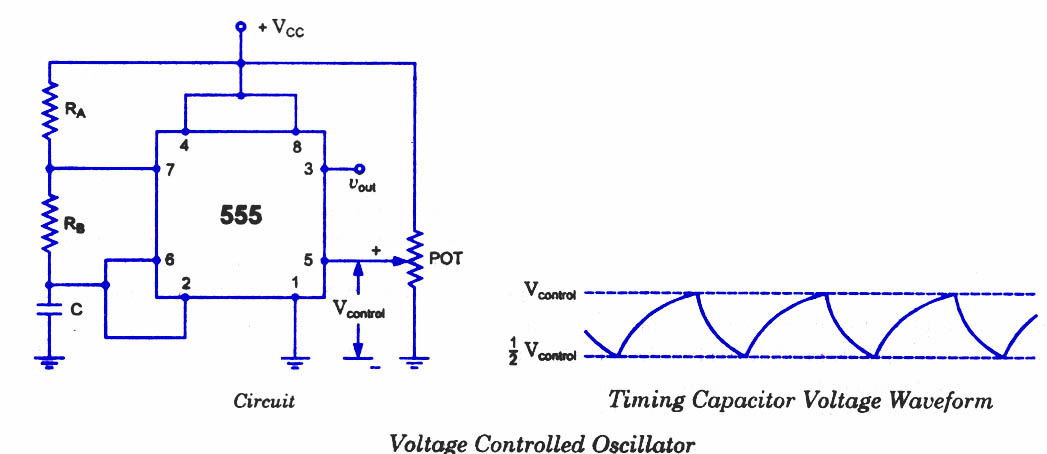
The circuit involving the pin 5 terminal typically functions within a timing application, such as a 555 timer configured in astable or monostable mode. The voltage control terminal provides an important means of adjusting the timing characteristics of the circuit. The internal voltage divider sets a default control voltage at approximately +2/3VCC, which is crucial for establishing the baseline operation of the timing mechanism.
When an external voltage is applied, either directly or through a potentiometer, the effective control voltage can be modified. This variation influences the behavior of the timing capacitor, which is essential for generating the desired output frequency. The capacitor's charge and discharge times are directly proportional to the control voltage; thus, an increase in control voltage leads to extended charge and discharge cycles, resulting in a lower output frequency.
The schematic representation of this circuit typically includes the timing capacitor connected to the threshold and trigger pins of the 555 timer, with the control voltage input at pin 5. The potentiometer can be depicted in series with the control voltage source, illustrating how the user can adjust the voltage applied to the terminal. Additionally, alternative sources for the control voltage, such as a transistor circuit or an operational amplifier, can be integrated into the schematic to showcase the versatility of this configuration.
Overall, this voltage control mechanism provides a flexible approach to modifying the timing characteristics of the circuit, enabling a wide range of applications in frequency generation and timing control. The capability to adjust the control voltage through various means enhances the functionality and adaptability of the circuit design in practical electronic applications.As discussed in previous blog posts, pin 5 terminal is voltage control terminal and its function is to control the threshold and trigger levels. Normally, the control voltage is +2/3VCC because of the internal voltage divider. However, an external voltage can be applied to thisterminal directly or through a pot, as illustrated in figure, and by a
djusting the pot, control voltage can be varied. Voltage across the timing capacitor is depicted in figure, which varies between +Vcontrol and ½ Vcontrol. If control voltage is increased, the capacitor takes a longer to charge and discharge; the frequency, therefore, decreases.
Thus the fre quency can be changed by changing the control volt age. Incidentally, the control voltage may be made available through a pot, or it may be output of a transistor circuit, op-amp, or some other device. 🔗 External reference
Related Circuits
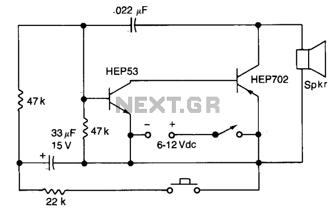
Closing the pushbutton switch initiates the siren, which then increases to a higher frequency. Releasing the switch causes the tone to decrease until switch S2 is closed again. The quality of the tone can be modified by altering the...
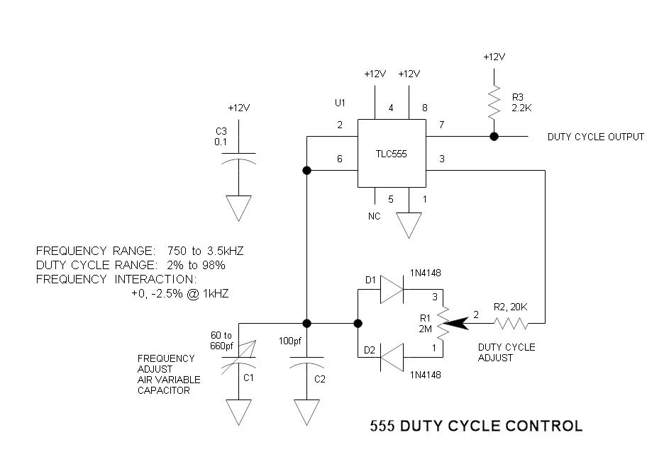
This is a simple oscillator circuit that varies the duty cycle over a wide range without affecting the frequency. It is a variation of the simple 555 astable multivibrator. The oscillator circuit utilizes the 555 timer IC configured in astable...

A simple Sump Pump Control Circuit using NE555. The described circuit utilizes the NE555 timer integrated circuit (IC) to create a control system for a sump pump. The NE555 can be configured in various modes, but for this application, it...
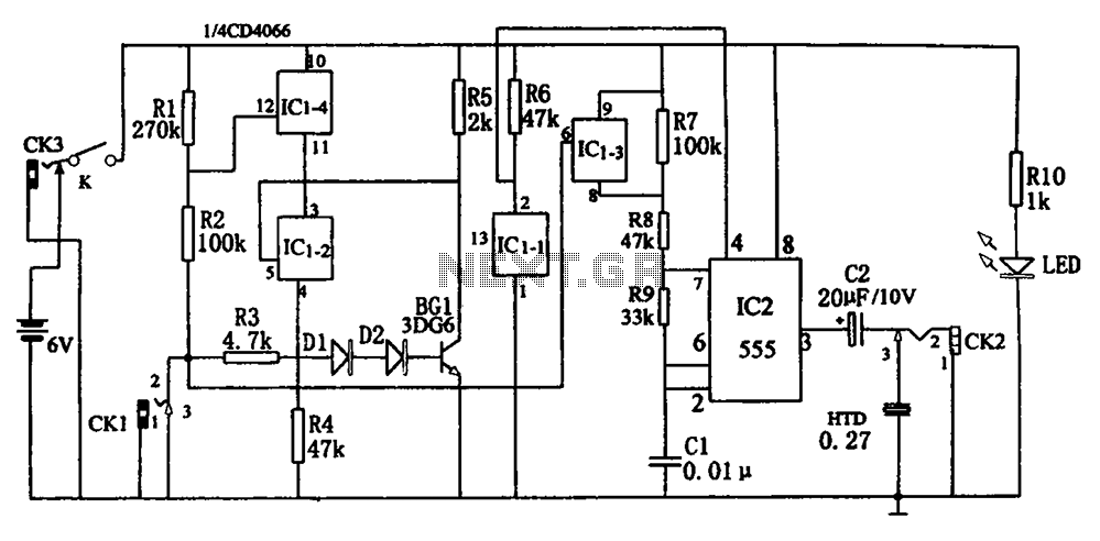
The circuit, illustrated in Figure five, employs a tri-state logic pen audio circuit. It primarily consists of a multivibrator, a four-way switch (CD4066, IC1), and several RC components. The multivibrator (555, IC2), along with resistors R7, R8, R9 and...
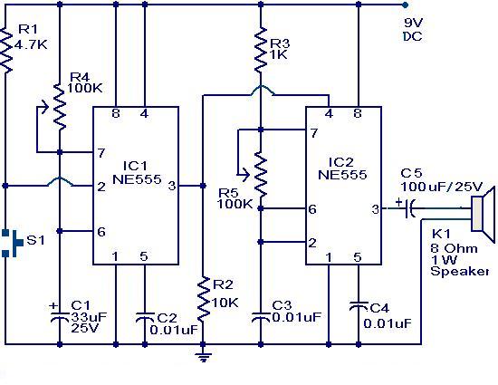
The primary component of this circuit is a doorbell utilizing two NE555 timer ICs. When the switch S1 is momentarily pressed, the speaker produces a bell sound, which is determined by the time period of the monostable multivibrator configured...
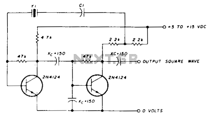
A capacitor in series with the crystal may be utilized to adjust the oscillator output frequency. The value may range between 20 pF and 0.01 µF, or it may be a trimmer capacitor, and it will approximately equal the...
Warning: include(partials/cookie-banner.php): Failed to open stream: Permission denied in /var/www/html/nextgr/view-circuit.php on line 713
Warning: include(): Failed opening 'partials/cookie-banner.php' for inclusion (include_path='.:/usr/share/php') in /var/www/html/nextgr/view-circuit.php on line 713