
Several gates as a crystal oscillator circuit

The described crystal oscillator circuits utilize various configurations of logic gates to generate stable oscillation frequencies. A crystal oscillator is a type of electronic oscillator that uses the mechanical resonance of a vibrating crystal to create an electrical signal with a precise frequency.
In the first configuration (Figure A), the circuit is designed to operate at 1 MHz, typically employing a simple inverter or buffer gate arrangement. The crystal is connected in a feedback loop, which determines the oscillation frequency based on its physical properties.
In Figure B, the 20 MHz oscillator circuit likely incorporates additional stages of amplification and filtering to maintain signal integrity at higher frequencies. This design may utilize more complex gate arrangements, such as a combination of NAND and NOR gates, to achieve the desired oscillation characteristics.
The variable oscillator circuit presented in Figure C allows frequency adjustment between 2 MHz and 20 MHz. This is typically achieved by incorporating variable capacitors or inductors in the circuit, which can alter the resonant frequency of the crystal oscillator. The use of a variable resistor in the feedback loop can also provide fine-tuning capabilities.
Figure D illustrates a variable oscillator circuit capable of functioning within a narrower frequency range of 5 MHz to 10 MHz. This configuration may involve a similar approach to the variable circuit in Figure C but is specifically optimized for a limited frequency range, potentially enhancing performance and stability within that band.
Lastly, Figure E depicts a dual-loop crystal oscillator circuit. This design often employs two feedback loops to improve phase noise performance and frequency stability. The dual-loop configuration can enhance the oscillator's ability to maintain a consistent output frequency, even under varying temperature and load conditions.
Overall, these circuits exemplify the versatility and precision of crystal oscillators in electronic applications, providing reliable frequency generation for a wide range of devices.It consists of several gates as a crystal oscillator circuit c Several gates as shown by a crystal oscillator circuit. FIG. (A) to l MHz crystal oscillator circuit, the figure (b) is 20 MHz crystal oscillator circuit, hide in (c) is variable 2-20 MHz crystal oscillator circuit, FIG. (D) is 5 --10 MHZ variable oscillator circuit diagram (e) of the dual-loop crystal oscillator circuit.
Related Circuits
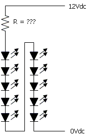
The color of the LED makes a significant difference. The type and size of the LED, such as 3mm or 5mm, and the power source are crucial factors to consider. More information is required for accurate calculations. A basic...
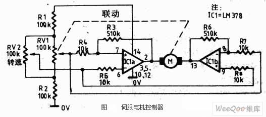
The servo motor is a type of traditional motor that serves as the execution component in automated devices. Its most significant characteristic is its controllability; when a control signal is applied, the servo motor rotates, with its speed being...
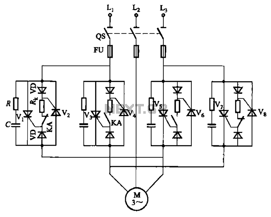
The circuit depicted in Figure 3-69 is designed for applications requiring frequent timing control for motor reversing operations. In this configuration, thyristors V1, V2, V7, and V5 are utilized for positive control of rotation, while thyristors V3, V4, and...
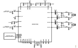
This is a typical stereo application circuit schematic of the ADAU1592, a 2-channel, bridge-tied load (BTL) switching audio power amplifier. The ADAU1592 can be utilized in flat panel televisions, PC audio systems, and mini-component applications. The ADAU1592 is designed to...
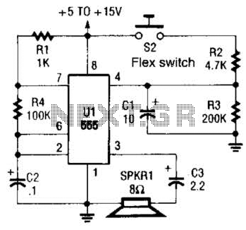
This is a cross-sectional diagram of a flex switch. They can be used as pushbuttons or even position sensors. This schematic diagram shows an oscillator, which is used as an alarm sounder, triggered by a flex switch. The flex switch...
Four observations regarding the Joule Thief AA battery LED circuit. The schematic of the LED circuit illustrates the power source (V1), which symbolizes a depleted battery with only 1 volt remaining and an internal resistance. The Joule Thief circuit is...