
Simple Analog Multiplier Circuit Using LM107
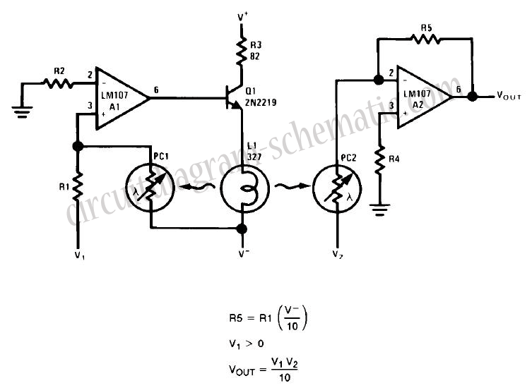
This analog multiplier circuit utilizes a combination of operational amplifiers and photoconductive elements to achieve its functionality. The core components include two operational amplifiers, A1 and A2, which serve distinct roles within the circuit. A1 acts as a control amplifier, monitoring the input voltage V1 and adjusting the resistance of PC2 accordingly. This feedback mechanism ensures that the resistance of PC2 is dynamically altered in response to V1, thereby influencing the overall gain of the system.
A2 serves as the controlled gain amplifier, where the gain is determined by the resistance of PC2 in relation to a fixed resistor, R5. The design allows for flexibility in output scaling, as R5 can be varied to achieve different output levels, making the circuit adaptable for various applications. The inverting nature of A2 means that the output voltage, VOUT, will be negative relative to the inputs, providing a straightforward relationship between the input voltages and the output.
The inclusion of the lamp, L1, plays a critical role in the circuit's operation. It not only provides the necessary light to activate PC2 but also acts as a current driver for the circuit. The design ensures that L1 is energized in accordance with the input signal V1, allowing for precise control over the circuit's response. The use of resistors R2 and R4 is crucial for maintaining accuracy by compensating for input offset currents, which can introduce errors in measurement.
Additionally, R3 is strategically placed to mitigate inrush current during the initial power-up phase, protecting the circuit components and ensuring stable operation. Overall, this analog multiplier circuit exemplifies a well-thought-out design that integrates various electronic components to achieve a specific function while allowing for adjustments based on application requirements.This circuit a simple analog multiplier, the circuit operation may be understood by considering A2 as a controlled gain amplifier, amplifying V2, whose gain is dependent on the ratio of the resistance of PC2 to R5 and by considering A1 as a control amplifier which establishes the resistance of PC2 as a function of V 1. In this way it is seen that VOUT is a function of both V1 and V2. A1, the control amplifier, provides drive for the lamp, L1. When an input voltage, V1, is present, L1 is driven by A1 until the current to the summing junction from the negative supply through PC1 is equal to the current to the summing junction from V1 through R1. Here is a schematic drawing : Since the negative supply voltage is fixed, this forces the resistance of PC1 to a value proportional to R1 and to the ratio of V1 to V -.
L1 also illuminates PC2 and, if the photoconductors are matched, causes PC2 to have a resistance equal to PC1. A2, the controlled gain amplifier, acts as an inverting amplifier whose gain is equal to the ratio of the resistance of PC2 to R5.
If R5 is chosen equal to the product of R1 and V-, then VOUT becomes simply the product of V1 and V2. R5 may be scaled in powers of ten to provide any required output scale factor. The circuit as shown gives an inverting output whose magnitude is equal to one-tenth the product of the two analog inputs.
Input V 1 is restricted to positive values, but V2 may assume both positive and negative values. This circuit is restricted to low frequency operation by the lamp time constant. R2 and R4 are chosen to minimize errors due to input offset current as outlined in the section describing the photocell amplifier. R3 is included to reduce in-rush current when first turning on the lamp, L1. 🔗 External reference
Related Circuits
A telephone remote control system allows users to perform various functions remotely using their phone. This system automates complex tasks, simplifying the development and operation of telephone systems. The telephone remote control system is designed to enhance user interaction with...
The installation of an electrical outlet in the refrigerator work light serves to enhance visibility of the refrigerator's interior while also improving the aesthetic appeal of the socket. The circuit is illustrated. Additionally, the circuit utilizes the secondary induced...
There are many ultrasonic pest repellent devices available on the market, but a major drawback is that their power output is low and their effectiveness suffers. Ultrasonic pest repellent devices utilize high-frequency sound waves to deter pests such as rodents...
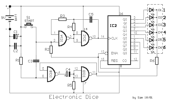
The circuit functions as a random number generator, producing numbers from 1 to 6. It features a line of LEDs, each corresponding to a number in the range of 1 to 6. When the push button S1 is pressed...
Fans can be controlled remotely with a switch that allows for speed adjustments, and this remote control can also be integrated with other household switches. Its primary feature is the use of a sub-transmission ultrasonic transmitter, which operates without...
Temperature sensor converter designed for use with a digital multimeter, capable of measuring temperatures from -40 °C to 110 °C. It features a state indicator and requires no calibration, utilizing the LM35 integrated circuit. The freezing point of water...
Warning: include(partials/cookie-banner.php): Failed to open stream: Permission denied in /var/www/html/nextgr/view-circuit.php on line 713
Warning: include(): Failed opening 'partials/cookie-banner.php' for inclusion (include_path='.:/usr/share/php') in /var/www/html/nextgr/view-circuit.php on line 713