
Simple Combination Lock
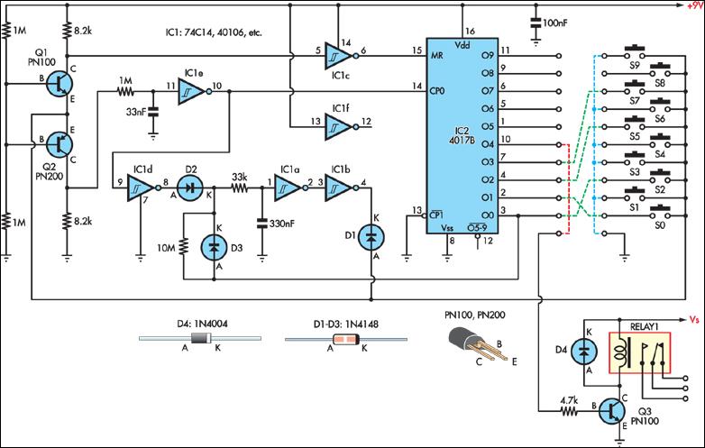
The combination lock circuit functions based on a series of logical states and transitions that are managed through the use of various integrated circuits and passive components. The core of the design revolves around the use of flip-flops and counters to track the input sequence of digits. Each switch press is debounced to prevent false triggering, ensuring that only deliberate presses are counted. The timing mechanism, facilitated by the capacitor and resistors, provides a window for user input while also ensuring that the system resets if input is not received within the specified timeframe.
The choice of components, such as the 330nF capacitor and 33kΩ resistor, is critical in determining the debounce timing and the overall responsiveness of the lock. The use of a relay driven by Q3 allows for the control of higher power loads, making the system versatile for various applications. The inclusion of protection diodes for inductive loads ensures that the circuit remains robust against back EMF, which could otherwise damage sensitive components.
This combination lock circuit is an excellent example of how digital logic can be used to create practical and secure applications, combining user input with electronic control to achieve reliable operation.This simple combination lock accommodates codes from 1-9 digits long, with the only restriction being that the same digit cannot be used twice. The circuit shows strapping for a 4-digit code, in this case "2057". Any unused switches are strapped to ground. When power is applied, the 330nF capacitor connected to pin 1 of inverter IC1a is discharged , holding it at a logic low level. The high output is inverted by a second gate (IC1b), with the result being a logic low on pin 4. This pulls Q1`s emitter low via D1, causing the transistor to conduct. The falling voltage on the collector then pulls the input of IC1c low, which in turn resets counter IC2. On reset, output O0 (pin 3) of IC2 goes high, charging the 330nF capacitor via D2 and the 33k © resistor.
If switch S2 is now pressed, Q2`s emitter will be pulled high and so Q2 conducts, applying a rising positive voltage to one end of the 1M © resistor. This resistor and the 33nF capacitor act as a switch "debounce" circuit, delaying the pulse through IC1e by about 33ms.
After the delay, the output of IC1e goes low. However, counter IC2 does not increment at this stage, since it needs a positive-going edge at the clock input (pin 14). When the switch is released, Q2 turns off, IC1e`s output goes high after the debounce period and the counter advances to the next state (ie.
O0 goes low and O1 goes high). When output O0 (pin 3) goes low, the 330nF capacitor starts discharging through the 33k © and 10M © resistors. This allows about 3s for the operator to press the next button. If no button is pressed within this period, IC1b`s output goes low, which pulls Q1`s emitter low and resets the counter via IC1c.
Hence the code entry must be restarted. When the second digit of the code is entered (0 in this example), Q2`s emitter is again pulled high. Q2 thus turns on and after the debounce delay, IC1e`s output goes low. When the switch is released, Q2 turns off, IC1e`s output goes high and the counter advances to state 2. Note that while the switch is pressed, IC1d`s output is high, recharging the 330nF capacitor and therefore resetting the 3s delay.
Thus, the operator is allowed another 3s to press the next digit. This process is repeated for each digit in the sequence. If the wrong switch is pressed at any point, IC2 is reset as described above. Conversely, if the correct code is entered, IC1 advances to state 4 (for our 4-digit example) on release of the fourth switch. Output O4 then goes high and turns on Q3 and relay 1. Q3 can handle up to about 300mA of load current. If more current is required, then either a Darlington or power Mosfet can be substituted. D4 is required if the load is inductive (eg, a relay, solenoid, etc). 🔗 External reference
Related Circuits
A useful feature of this circuit is that the frequency can be changed by modifying the capacitor value. A switch can be added to select between various frequencies. This circuit utilizes a capacitor in conjunction with an oscillator to determine...

The circuit timer with a musical alarm utilizes a well-known CMOS oscillator/divider integrated circuit (IC1). Although this circuit operates at 9V, its standby current drain is minimal. The time delay of the timer circuit can be adjusted by modifying...
The cut on a fader is fundamentally different from a transform. It is not an instantaneous on/off switch; rather, it features a gradual slope that can range anywhere from a few hundred microseconds to tens of milliseconds. This duration...

The clock displays time in 5-minute intervals, with adjustable hour and minute settings. There is no alarm feature or AM/PM indicator. The clock face is constructed from two pieces of linoleum glued together for added thickness, though floor tiles...
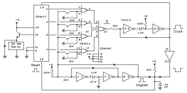
The digital lock utilizes four common logic integrated circuits (ICs) to manage a relay activation by inputting a four-digit code via a keypad. The initial four outputs from the CD4017 decade counter (pins 3, 2, 4, and 7) are...
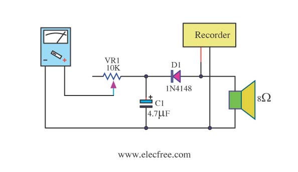
Expensive stereo systems generally feature VU meters that help indicate maximum power levels to prevent overloading. However, typical radio tape players do not include VU meters. A potential solution involves using a multimeter as a replacement. This can be...