
Simple Deadband Generator Targets Push-Pull Drivers

In a typical push-pull driver configuration, the NPN and PNP transistors function as complementary devices to drive a load. The operation is controlled via square-wave signals applied to the bases of the transistors, enabling efficient switching. The challenge arises from the inherent differences in the turn-on and turn-off characteristics of the transistors, which can result in simultaneous conduction, known as cross conduction, during the transition phase. This phenomenon can lead to excessive current draw from the power supply, potentially damaging components and reducing overall efficiency.
To mitigate this issue, a circuit can be designed to introduce a deadband between the control signals V1 and V2. By incorporating a Schmitt-trigger inverter, such as the 74HC14, the circuit can provide hysteresis, which enhances noise immunity and provides clean transitions. The use of diodes allows for the adjustment of timing delays for both the rising and falling edges of the output waveform. The deadband duration is primarily influenced by the RC time constant, which can be tailored to suit specific application requirements.
The waveform characteristics, as depicted in the accompanying figures, illustrate the effectiveness of the deadband in preventing cross conduction. The flexibility of this circuit design permits the use of various transistor types in the push-pull arrangement, thus eliminating the need for closely matched pairs. This not only simplifies the design process but also reduces costs associated with sourcing matched transistors, making the circuit more accessible for various applications in electronics.In typical push-pull driver applications, the npn-pnp transistor pair is alternately turned on and off using a square-wave signal. A simple driver circuit uses an inverter between the V1 and V2 inputs to toggle the output transistors.
However, mismatched turn-on and turn-off characteristics of the output transistors can cause cross conduction during the transition periods ( Fig. 1 ). This results in high current surges being drawn from the power supply. The simple circuit shown in Figure 2 can be used to introduce any desired amount of deadband time between V1 and V2 control pulses. The circuit employs a Schmitt-trigger inverter IC, the 74HC14. With the diodes, different time delays can be obtained for the rising and falling edges of the drive waveform.
The deadband is determined by the RC time constant. The waveforms in Figure 3 are self-explanatory. Using this circuit, any type of transistors can be utilized for the push-pull circuit, eliminating the effort and expense required to obtain matched transistors. 🔗 External reference
Related Circuits
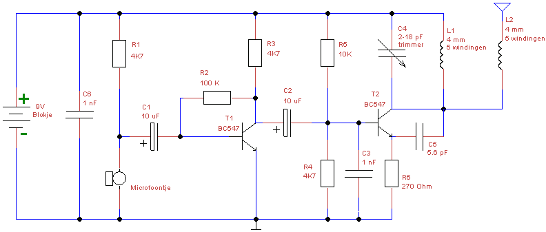
This is a simple design of a small FM transmitter bug that is ideal for transmitting and eavesdropping purposes. Due to its high sensitivity, it can even pick up the ticking of a clock. The estimated range is approximately...
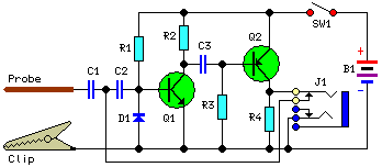
This simple circuit generates narrow pulses at a frequency of approximately 700-800 Hz. The pulses, which contain harmonics extending into the MHz range, can be injected into audio or radio-frequency stages of amplifiers and receivers for testing purposes. A...

This project presents a useful device for the beach, intended to deter individuals from touching personal belongings left on a towel while swimming. It can also be employed in an office or workshop setting. The circuit, compact in size...

The circuit utilizes a dual operational amplifier integrated circuit (IC), specifically the 1458, which contains two separate op-amps within a single package. In this configuration, the first op-amp functions as a voltage follower, directing its output to charge capacitor...
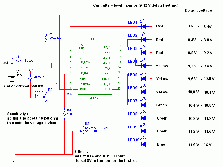
This circuit utilizes the widely available LM3914 integrated circuit (IC), which is straightforward to operate and does not require external voltage regulators due to its built-in voltage regulation capabilities. It can be powered from various sources. When the test...
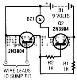
A common collector amplifier drives a 2N3904 switch to sound alarm BZ1. The wire leads to a water sensor or sump pit, level switch, etc. It is used to allow the alarm to operate and be mounted in a...