
Simple JFET Preamp
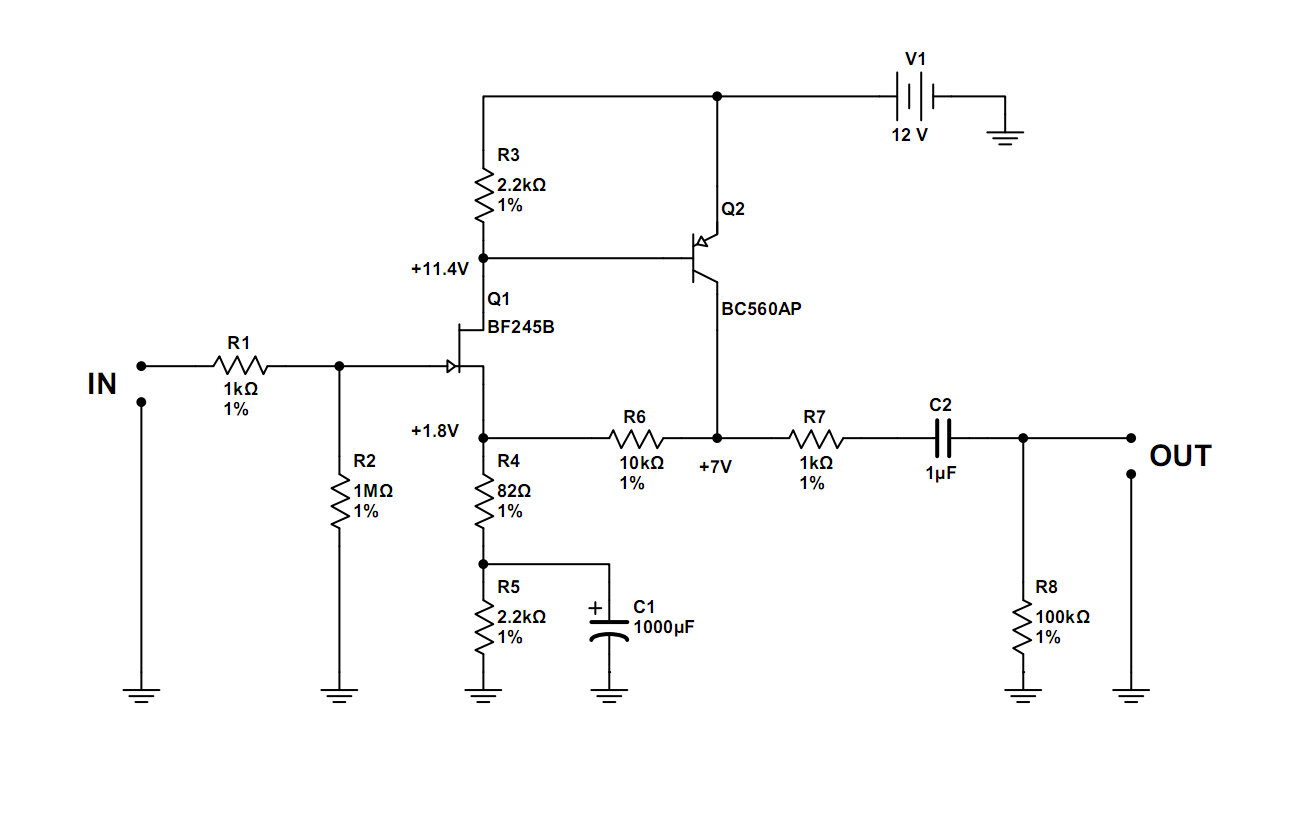
The described JFET preamplifier circuit is designed to enhance weak signals, making it an essential component in various audio and signal processing applications. The circuit utilizes a JFET (Junction Field Effect Transistor) as the primary amplification element, which is favored for its high input impedance and low noise characteristics. The connection of the gate to ground through R2 ensures that the JFET operates in its optimal biasing region, facilitating effective signal amplification.
The circuit's configuration includes feedback mechanisms through R4 and R6, which stabilize the gain and improve linearity by reducing distortion. The feedback loop allows for better control over the gain of the amplifier, ensuring that it remains consistent across varying input signal levels. The use of resistors R1 and R7 as protective elements is critical for safeguarding the circuit from potential damage due to excessive voltage or current, which could occur during fault conditions.
The high input impedance, primarily determined by R2, allows the preamp to interface effectively with high-impedance sources, such as microphones or piezoelectric sensors, without loading them down. The low noise performance of the JFET further enhances the circuit's capability to maintain a high S/N ratio, making it suitable for applications where signal integrity is paramount.
Overall, the design of this JFET preamp exemplifies the principles of low-noise amplification and high input impedance, making it a valuable tool in the field of electronic signal processing. The careful selection of component values and configurations ensures reliable performance and protection against common electrical faults.The following is an example for a very simple and high quality JFET preamp. You can use this to amplify a very low signal sources. FET transistors are usually not used independently in preamplifiers. In most of the cases they are paired with bipolar transistors. R2 automatically sets the bias for Q1 in a way similar to a tube circuit. This resisto r tides the gate of Q1 to ground and sets its potential. Source`s potential is higher than ground by the voltage across R4 and R5. In other words the gate is more negative then the source. The gate-source transition represents a normal PN junction. Usually this junction is tied in opposite direction, which explains the relatively high input impedance (more than 109 ©). Basically the input impedance of the circuit is set by R2 and in this case it`s around 1M ©. R4 and R6 form an AC negative feedback. R1 and R7 serve as over voltage limiters and over current limiters in case of short circuit at the input or output.
Besides their high input impedance, the FET transistor preamps have one more advantage. This is the very low noise. This means that we can easily design a stage with high S/N ratio. Considerable deviations from these values will cause the stage not to perform as it should be. 0V at the collector of Q2 means that there is a break into collector-emitter junction while 12V means there is a short between those two outputs. The voltage at the base of Q2 is equal to one voltage drop of a normal junction which is about 🔗 External reference
Related Circuits
The 555 timer is recognized as one of the most versatile and widely used integrated circuits globally. One of its potential applications is as a simple inverting Schmitt trigger. The 555 timer can be configured in various modes, including monostable,...
A simple preamplifier circuit is often required, utilizing a few components for ease of construction. This circuit employs an operational amplifier, specifically the Motorola TCA5550, which features a dual amplifier configuration. It provides outputs for adjusting volume, balance, treble,...
The circuit was designed to create a modular Class A buffer preamplifier to isolate stages in an audio circuit. BF245 is a general-purpose N-Channel JFET used in this design. The modular Class A buffer preamplifier serves as an essential component...
The loads consist of two or more solenoids connected in parallel, sharing a 12V supply. Each solenoid is individually switched to ground through the vehicle's ECU. The objective is to detect when any one of the circuits closes, ensuring...

When the phototransistor is struck by infrared (IR) light, it begins to conduct, causing the voltage across a 1 MΩ resistor (chosen arbitrarily) and the phototransistor to drop from VCC to lower values. When this voltage falls below VCC/3,...
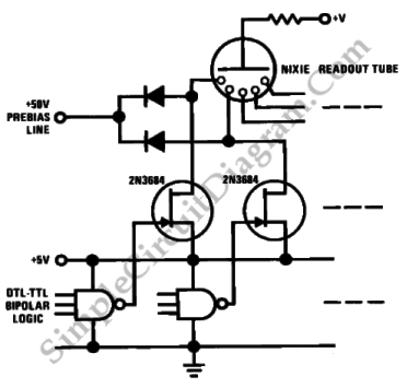
This is a driver circuit for a nixie tube. The circuit utilizes the 2N3684 transistor as the nixie tube driver due to its Vp rating of 2-5 volts, which ideally matches TTL-DTL logic levels. The nixie tube driver circuit is...