
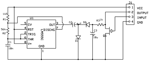
Simple Pyro RF Receiver (27 MHz) Circuit
The circuit is designed to operate as a regenerative receiver, which utilizes feedback to enhance sensitivity. The antenna captures RF signals, which are processed by the regenerative receiver front-end. This section typically includes a transistor or operational amplifier configured to achieve regenerative feedback, allowing for the amplification of weak signals. The tuning components, L2 and C2, form a resonant tank circuit that is critical for selecting the desired frequency of 27.145 MHz. Proper tuning is essential to ensure that the receiver is sensitive to the intended frequency while rejecting others.
The two amplifier stages are configured to provide additional gain, transforming the signal into a clean square wave suitable for digital processing. These stages may consist of common emitter or common source amplifiers, which are effective for achieving the required gain while maintaining signal integrity. The output from these amplifiers is fed into the 555 timer, which is configured in a monostable or astable mode depending on the desired output characteristics. The internal comparators of the 555 timer compare the input signal to a reference voltage, enabling it to switch the output state, thereby activating the green LED as an indication of signal detection.
The PCB layout is an important aspect of the design, affecting both performance and manufacturability. The placement of components should minimize trace lengths to reduce inductance and capacitance, which can degrade performance, particularly in RF applications. The ground plane serves to provide a low-resistance return path for signals, enhancing overall circuit stability. The choice of trace width is critical; while thicker traces may be easier to work with during construction, smaller traces can reduce parasitic effects in high-frequency designs.
In summary, this schematic represents a functional regenerative receiver capable of detecting and processing RF signals, with careful consideration given to component selection, circuit layout, and PCB design principles to optimize performance.The schematic for this project flows naturally from left to right. Beginning at the antenna and the regenerative receiver front-end, then flowing through the amplification stages and then into the 555 timer. This is a very common regenerative receiver front-end that you can find in circuits all over the web.
I tailored the parts used to what I ha d laying around, generally you can tweak part values a little bit, with the exception of L2 and C2 which are your tuning circuit (tank circuit) for 27. 145 MHz. Two amplifier stages exist in the middle of the schematic. They are used to `rail` the signal back to its square-wave digital form of either +5v or +0v. I`m pretty sure that these amplifiers could be tweaked to get better performance, however the current design should work well enough for our requirements.
The amplified signal makes its way to the 555 timer in the form of its original square wave where this 555 timer uses the voltage detected with internal comparators to create an output that turns on the green LED. The board layout for this project was done in a similar way as the schematic. The front-end receiver can be found on the top left side of the board, then the amplifier stages on the top right and finally the 555 timer and our output LEDs at the bottom right side.
Just like with the transmitter, it`s pretty important to have a ground plane for the receiver to act as a better antenna and keep extra noise out of the circuit. A solid ground plane would be very ideal, however for simplicity`s sake we`ll use a chopped up one with traces.
I just chose a nice thick width that would transfer over nicely when building the PCB, however smaller trace widths seem to be a better choice when designing RF circuits. but at these low frequencies I don`t believe there will be any performance benefit. My PC board had extra space so I plugged in PyroElectro. com. You`ll notice the text is backwards, this is because during the toner transfer process, a bottom layer is technically printed out backwards, but once on the PCB it reads correctly.
🔗 External reference
Related Circuits
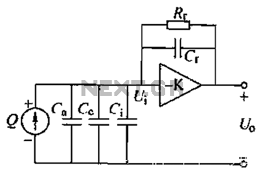
A charge amplifier is an effective device for measuring punch hits. This amplifier utilizes a negative feedback capacitor in conjunction with a high-gain operational amplifier. The amplifier operates with minimal shunt, relying primarily on the feedback capacitor's charge (q...
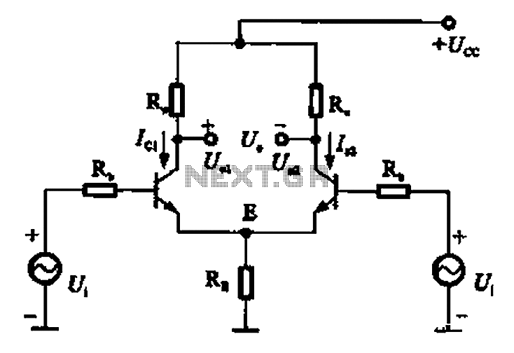
The common mode signal of an emitter-coupled differential amplifier circuit assumes that two equal small increases of the same polarity signal, referred to as the common mode signal, occur simultaneously. This results in an increase in the potential at...
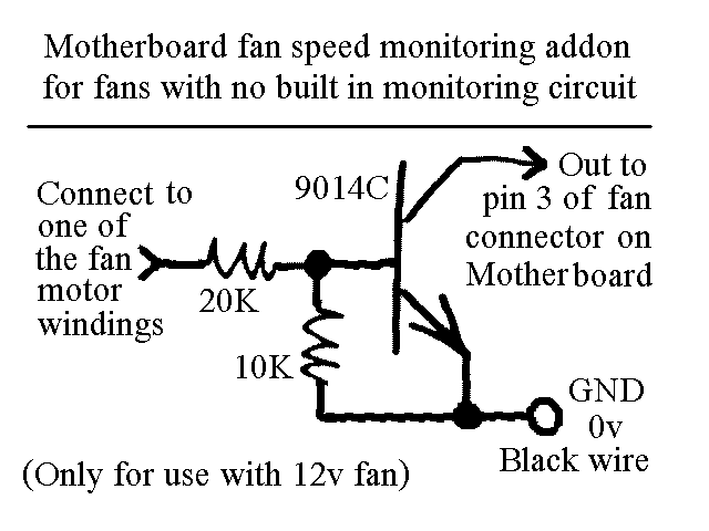
You will find this identical circuit inside most 3 wire computer fans with speed monitoring output to the motherboard. Peel off the sticker from the fan hub in order to access a motor winding pin for connecting up the...
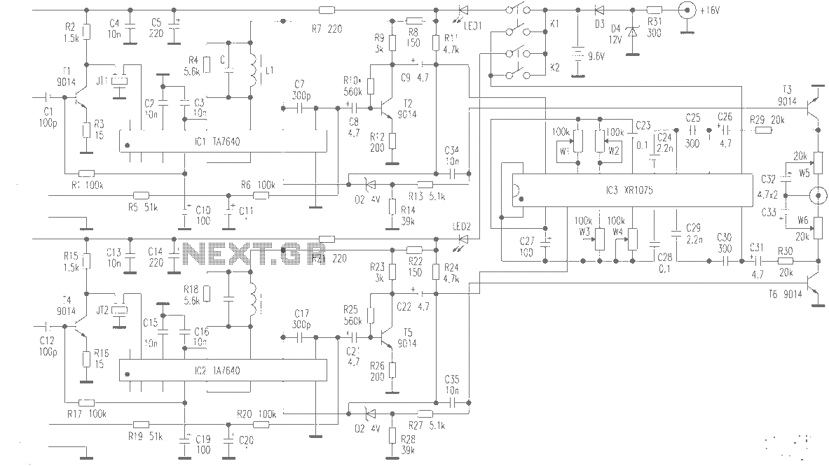
The production of high-quality wireless microphones is a common aspiration among enthusiasts, but achieving a high-performance receiver is challenging. This project explores the use of salvaged FM radio cassette players to enhance an XR1075 audio processor, leading to the...
Our programmable MP3 player has an interface to an LCD with a HD44780 controller. These are alphanumeric LCDs with one to 4 lines of text and 16 to 40 characters per line. However, these LCDs (and LCDs in general)...
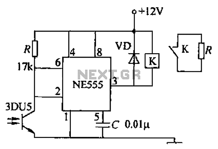
A transmitting circuit powered by an infrared light-emitting diode emits light. The receiving circuit, shown in the figure, utilizes a transistor (3DU5) to receive the infrared light and output the received signal. The signal is sent to terminal 3...