
Simple RF Signal Generator

The Franklin oscillator circuit is an efficient design that leverages FET technology to produce stable RF signals suitable for various applications, including antenna analysis. By employing a common drain configuration for the first stage, the circuit achieves high input impedance, which is crucial for interfacing with sensitive measurement equipment without affecting the circuit's performance. The use of a common gate configuration in the second stage allows for effective feedback while ensuring that the oscillator's output remains robust and stable.
The choice of components is paramount; employing high-frequency capable transistors can significantly enhance performance, particularly in applications that demand operation above 30 MHz. The transformer design is also critical, as it not only matches impedance but also influences the overall bandwidth and efficiency of the oscillator. The winding technique, such as bifilar winding on a ferrite core, plays a role in reducing parasitic capacitance and improving signal integrity.
In summary, the Franklin oscillator presents a practical solution for RF signal generation, characterized by its simplicity and effectiveness. The design considerations detailed herein provide a roadmap for successful implementation, ensuring that the oscillator meets the demanding requirements of modern RF applications.This circuit came out of some work I did for the two antenna analysers which are described elsewhere on this site. Those instruments both include an RF signal generator. This is used as the signal source to drive the impedance bridge and detectors used to measure impedance.
Those instruments ended up with somewhat different oscillator designs due to other conflicting design issues. The signal generator outlined here is much simpler, and quite easy to build. The design is based around the Franklin oscillator configuration. This is perhaps not as well known as other types of oscillator, such as the Colpitts or Hartley. This is also called a "source-coupled FET oscillator" in some books and articles. This oscillator, shown in outline form above, uses two active devices. Some designs I`ve seen use two capacitors to couple into and out of the resonant circuit, but in practice, only a single capacitor is actually required with this circuit. This simple two-FET circuit forms the heart of this Franklin oscillator. It`s really a two-stage amplifier with feedback. A common drain FET first stage is followed by a common gate FET second stage. The first stage gives high gain with a high input impedance to minimise loading on the oscillator`s tuned circuit components.
The coupling capacitor is usually a small value, typically less than 10 pF. The second common gate FET stage has no voltage gain. The low input impedance of this stage permits the stage to be fed from the first FET`s source resistor. The output of this stage provides the feedback loop to permit oscillation, and since the output impedance of this stage is high, this minimises loading again on the oscillator`s tuned circuit.
This is enhanced to some extent by the use of an RF choke which is a high impedance at RF but with low DC resistance for supplying DC to the second FET. This oscillator will operate, with suitable devices, beyond 3 GHz. This is discussed in more detail in Reference 1. The nice feature of this arrangement is that there is minimal additional capacitance in parallel with the tuned circuit.
This maximizes the tuning range possible from the variable capacitor tuning the oscillator and can, if desired, minimise the number of oscillator ranges required. In the prototype, the entire tuning range of 450 kHz to 60 MHz is covered in just three ranges. The RF choke presents something of a challenge. RF chokes do not present the desired perfect high impedance across the entire RF range covered by the oscillator!
Some minor variation of oscillator output levels can be traced to this part. If you experience problems when building this oscillator, try a different brand or value of RF choke, or even a pair of RF chokes in series or in parallel. The oscillator`s output is taken from the source resistor of the first stage, and goes to a cascade buffer stage using a pair of transistors.
Although Q3 and Q4 are shown as BC548B transistors, performance will be somewhat improved above 30 MHz if better transistors such as the 2N2222 are used. The cascade arrangement of Q3 and Q4 mirrors the circuit of the first stage to some extent. There is no feedback in this buffer stage, of course, and the output is delivered via a 4:1 wideband transformer.
If a little more output is desired, it is possible to wind this transformer as a 9:1 transformer using three windings rather than two. In the prototype, I made this transformer by winding 7 bifilar wound turns onto a small ferrite bead.
(Right click on the diagram to the left to see the full details) For those needing a little more information, first get a ferrite bead. These are about 4 to 5 mm long and about 3 mm in diameter. Ferrite beads have a single hole through the centre, so they look like miniature cylinders. Some seem to have smaller holes than others, so if you have a choice, use the bead with the largest hole.
This makes winding the transformer a little easier. Now ge 🔗 External reference
Related Circuits
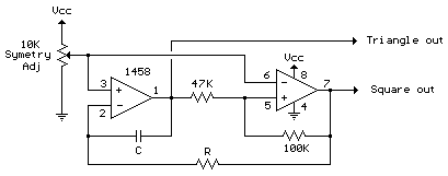
A simple triangle and square wave generator utilizing a common 1458 dual op-amp, capable of operating from very low frequencies up to approximately 10 kHz. The time interval for one half-cycle is determined by the product of resistance (R)...
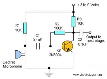
This straightforward circuit offers substantial amplification for weak audio signals, such as those from an electret microphone. It can be utilized in conjunction with an RF oscillator to create a highly sensitive RF transmitter. The audio microphone preamplifier circuit...

Noise level measured into 75ohm 3.1kHz BW using Siemens D2006 level meter: -80dBU (77.5mV) from zero to 1MHz and drops 3dB on 17MHz. Decrease the first coupling capacitor (68nF) to 10nF to increase the lower limit to 50kHz. The...
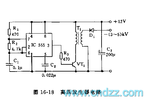
The high voltage generator depicted in figure 16-18 utilizes the 555 timer IC as its primary component. The oscillating voltage produced is enhanced through a step-up transformer. The astable multivibrator configuration comprises the 555 timer along with resistors R1...
The audio source will be a line-level audio signal ranging from -2V to +2V AC, which will be passed through a 220µF coupling capacitor followed by a two-pole low-pass filter (RC). The signal will be processed by an Analog-to-Digital...
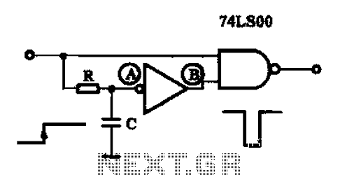
A single pulse signal generating circuit is designed to produce a one-shot pulse output. This circuit can be utilized in applications requiring a digital reset signal or to halt a signal. It operates as a non-synchronous differential circuit. The single...