
DC biasing audio signal

The circuit design begins with a line-level audio signal that oscillates between -2V and +2V AC. This signal is first processed through a coupling capacitor rated at 220µF. The primary function of this capacitor is to block any DC component of the signal while allowing the AC component to pass through. Following the coupling capacitor, the signal is directed to a two-pole low-pass filter, which is implemented using resistors and capacitors in an RC configuration. This filter is essential for attenuating high-frequency noise that may interfere with the desired audio signal.
The processed signal is then fed into an ADC, which will convert the analog audio signal into a digital format suitable for further processing, such as calculating beats per minute (BPM). The design incorporates a FET-BJT preamplifier circuit, where two versions are considered. The second version is recommended due to its ability to maintain a stable bias point, which minimizes the introduction of noise from the power supply into the audio signal. This is particularly important in environments with significant electrical noise, such as in model aircraft, where motors and servos can introduce unwanted interference.
In the second preamp configuration, the output voltage is shifted upward by 2.5V, which provides a suitable DC bias level for the ADC. The resistor on the input side of the coupling capacitor ensures that the voltage at this point remains at 0V DC, preventing any audible pops during the connection process. Additionally, the output resistor biases the output side of the coupling capacitor to the DC voltage level.
For generating the DC bias voltage, a voltage divider can be employed along with a filtering capacitor to mitigate power supply noise. It is crucial to be aware of potential crosstalk if multiple signals share the same bias point; using a larger bias capacitor can help reduce this effect. Similarly, while larger coupling capacitors can enhance low-frequency response, excessively large capacitors may result in slower charging times when the circuit is powered on, which could affect the overall performance.
In summary, this circuit design effectively combines audio signal processing with noise reduction techniques to ensure a clean and reliable input for the ADC, suitable for applications requiring accurate BPM measurements in electrically noisy environments.My audio source will be a Line Level Audio -2V to +2V AC passed through a 220uF coupling cap and then a low pass filter(RC, 2 pole). The signal will be read by an ADC another one that i have seen is I don`t quite understand this FET-BJT preamp circuit And the schematic is for a pre-amp, and there are 2 versions and both add a bias.
using the second one looks like it will work best for my application, using something like this- is there any other improvements I can make other then Stable Vref/power rails. The signal is going to be read by an ADC, for a BPM counter(beats per min) And Kellenjb you are correct coupling cap and not decoupling - fixed jsolarski May 18 `11 at 12:31 As a note: I use the first solution with no problems but my circuit is definitely not a high fidelity one as it is on a model aircraft with lots of other noise (motors, servo, wind etc.
) Thomas O May 18 `11 at 16:11 Don`t use the first circuit. Any noise or spikes on the power supply will be mixed with your signal. Because the bias point is connected directly to the signal, you can`t filter out power supply noise without also filtering out the signal. Do use the second circuit. It produces a mid-point voltage that is tightly coupled to ground, so the DC component is half the supply, but the AC component (noise and spikes) is filtered out by the capacitor.
That`s not a complete circuit, though, you still need to connect it to your signal. The output is the same as the input, just shifted upward by 2. 5 V. The resistor on the input ensures that the input side of the capacitor is at 0 VDC, to prevent pops during connection. The resistor on the output side of the AC coupling cap biases that side to the DC bias voltage. If your circuit already has a clean, low impedance DC bias voltage source, connect to that. Otherwise, you can use circuit #2 to generate the bias, like this : The DC bias voltage is produced by a voltage divider and capacitor to filter out power supply noise.
Note that if you use the same Vbias point for multiple signals, they can crosstalk through this point. Larger bias cap reduces crosstalk. Larger coupling capacitor improves low frequency response. But make them too large and they`ll take a long time to charge when you flip the power switch. 🔗 External reference
Related Circuits
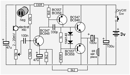
The following circuit presents a Mini Audio Amplifier Circuit Schematic Diagram. Features include a power consumption of less than 3mA, a small output, and the use of a push-pull configuration. The Mini Audio Amplifier Circuit is designed to amplify low-level...
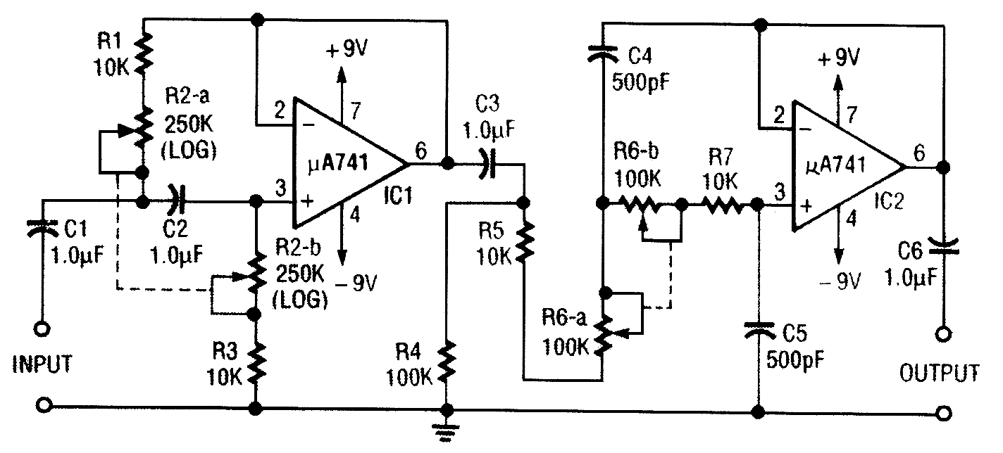
This circuit is a variable audio bandpass filter that features a low cutoff frequency adjustable from approximately 25 Hz to 700 Hz and a high cutoff frequency adjustable from 2.5 kHz to over 20 kHz. The roll-off rate is...
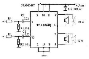
This car audio amplifier provides an output of 40 watts when connected to a 2-ohm speaker. The amplifier circuit delivers a power output of 40 watts per channel at a 2-ohm load and 22 watts at a 4-ohm load....
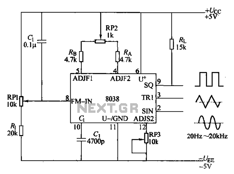
The audio function generator integrated circuit ICL8038 is capable of producing square waves, triangle waves, and sine waves. The electrical resistance and potentiometer RP1 are utilized to determine the 8-pin DC potential Ua, which is typically set to 2Ucr/3....
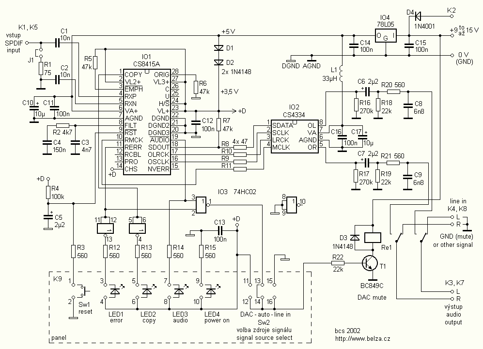
The described device is used to convert the digital signal format S/PDIF (AES3) to analog. It can be used for any device with uncompressed digital audio output (desktop CD or DVD, minidisk, sound card PC CD-ROM). Separate transmitter can...
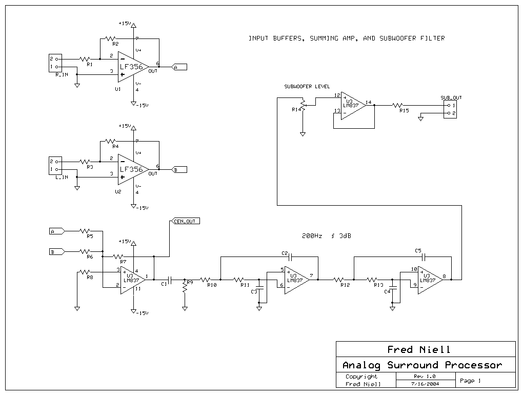
The overall block diagram of the system shows that audio input enters from the left and undergoes various processing steps including summation, differencing, multiplication, delay, and filtering. The output consists of five discrete audio channels along with one low-frequency...