
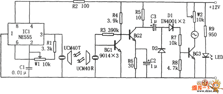
Single Channel Universal Infared Switch by 555 Timer
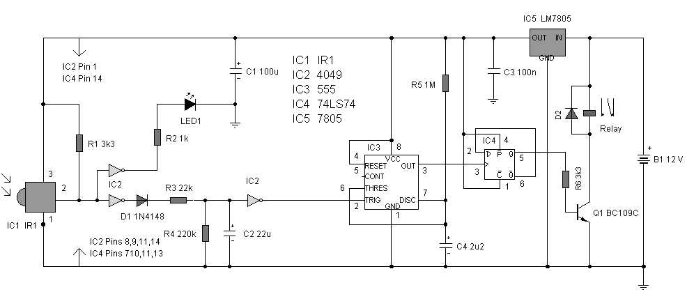
The universal infrared switch circuit is structured around several key components that work together to ensure reliable operation. The TSOP1738 receiver module serves as the heart of the infrared detection system, converting incoming infrared signals into electrical signals that can be processed by the circuit. This module is designed for optimal sensitivity and immunity to interference, making it suitable for various environments where ambient light may fluctuate.
The circuit utilizes a CMOS inverter, which is pivotal for signal processing in this application. CMOS technology offers low power consumption and enhanced noise immunity, making it ideal for battery-operated remote control applications. The inverter's output state, controlled by the received infrared signal, is crucial for the operation of the relay that powers connected devices.
The timing elements of the circuit, specifically the resistor-capacitor (RC) combination, play a critical role in determining the response time of the switch. The time constant, defined by the product of R3 and C2, dictates how long the circuit remains in the ON state after the button is pressed. This design ensures that the switch does not inadvertently activate due to brief signal fluctuations, providing a stable control mechanism.
The inclusion of a 555 timer in monostable mode adds a layer of functionality, allowing the circuit to maintain its output state for a predetermined duration, defined by R5 and C4. This feature is particularly beneficial for applications requiring a precise timing control for device activation.
Overall, the universal infrared switch circuit exemplifies a well-thought-out design that integrates various electronic components to achieve reliable remote control functionality. Its adaptability to different remote control systems and the ability to interface with various electronic loads make it a versatile solution for infrared switching applications.The circuit was designed to produce a universal infrared switch with a single channel and ON/OFF feature to operate in 36 kHz to 38 kHz in the form of a remote control. Infrared a portion of the electromagnetic spectrum found between the microwave/radio waves and visible light region; contains a frequency range from 300 GHz to 400 THz and wave
length from 1 mm to 750 nm TSOP1738 miniaturized receivers for standard IR remote control systems having the IR filter designed with epoxy package, the preamplifier and PIN diode assembled on lead frame, and the demodulated output signal directly decoded by a microprocessor CMOS inverter a circuit containing complementary MOS transistor having either low or high input voltage with either high and low output voltage respectively The receiver side of the circuit is using the infrared that can be substituted by TSOP1738 to convert the received modulated infrared signal into electrical signal. It has features such as CMOS and TTL compatibility, improved shielding against electrical field interference, high sensitivity, high level of immunity to ambient light, integrated oscillator, 5V output, amplifies and receives the infrared signal without any external component, and encloses the preamplifier circuit and photodetector in the same housing.
For the relay to operate this universal switch, the button should be pressed for about 1. 5 seconds as established by the resistor R3 and capacitor C2. Until doing a reset, the circuit will keep on at this condition. The reset happens by pressing any button for a short period in the remote handset. The buttons could be any type and be used in any remote control. Other electronic components, like a lamp, can be connected to the relay for as long as the rated current and voltage can be handled by the relay contacts. IC1 functions as the infrared module that is responsible for buffering and receiving the IR modulated signal or pulses.
The transistor-transistor logic (TTL) handles the standard output since it uses less power and is less sensitive from electrostatic discharge damage as compared to CMOS. The output is kept high by resistor R1 in the absence of signal. LED1 acts as a visible switching aid which is driven by one gate of a CMOS inverter, which consists of gates implementing logical negation of the input.
The time constant circuit consists of D1, C2, R3 and R4 where the signal is buffered by another gate. The capacitor C2 discharges through R4 while it charges through R3. Through the low output impedance of the CMOS buffer, the quick discharge is avoided by D1. If IR1 will be replaced by TSOP1738, then resistor R4`s value need to be increased from 220K ohms to 470K ohms.
The RC time constant is calculated by the product of resistance and capacitance as this denotes the charging time by a capacitor. Only 63% of the voltage supply will be charged by a capacitor at one RC circuit while 99% of capacitor charging would require 5 RC circuits.
The logic threshold of the CMOS inverter in this circuit is the reference point of charging for the capacitor. The input threshold is around 3. 6V since the power supply is 5 Volts. This is equivalent to 3 RC circuits that will last for 1. 5 seconds. CMOS inverter triggers the 555 timer upon reaching the threshold and will function as a memory circuit or flip flop where it will stay in two states of high output and low output.
As an illustration, although not the actual circuit, the figure shows a simulation of output pulse, filtering and received pulses. It only displays a spice simulation during the duration of 555 monostable with high pulses. The figure shows jiggered edges of the further buffered pulses which are produced by the IR modulated data.
The jiggered edges are removed by the 555 timer functioning in monostable mode in IC3. The output of the pulse duration is determined by R5 and C4. To activate the bistable IC4, a clean output is required 🔗 External reference
Related Circuits
This is a circuit of a Clap Triggered Switch. When the circuit detects a tap, a short whistle, or a clap, it will toggle the LEDs. Resistors of 33k and 5.6k are used to charge the circuit. The Clap Triggered...
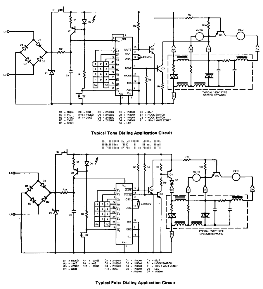
The XR-T5990 single-chip pulse/tone dialer is a silicon gate CMOS circuit that performs both pulse and tone dialing functions. It is designed to operate directly from the telephone line or from a separate small power supply. Additionally, a 17-digit...
Without the specified delay, the circuit could malfunction or even sustain damage. A capacitor, which is a crucial component of the circuit, is positioned at the other end of the base resistor rather than directly connected to the base...
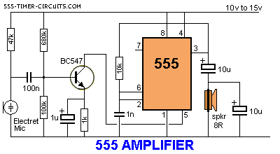
The 555 timer can function as an amplifier, operating similarly to pulse-width modulation. The component values lead the 555 to oscillate at approximately 66 kHz, a frequency to which the speaker does not respond. Instead, the speaker reacts to...
This circuit provides a visual 9-second delay using a 7-segment digital readout LED. When the switch is closed, the CD4010 up/down counter is preset to 9, and the 555 timer is disabled with the output held high. When the...
The image depicts an ultrasonic liquid level indicator circuit. This circuit consists of an ultrasonic transmitter circuit and a receiver circuit. The ultrasonic transmitter circuit includes a 555 timer, resistor R1, variable resistor W1, capacitor C1, and the ultrasonic...