
Single-chip TRMS Power Measurement System AD8362 Demodulation
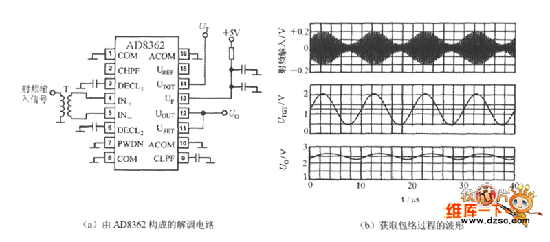
The AD8362 is a versatile RF envelope detector and demodulator that operates effectively in various applications, including communication systems and signal processing. The primary function of the UTGT side is to perform envelope detection, which is critical for recovering the original information signal from a modulated carrier wave.
In the demodulation circuit, the input signal, which is a modulated 100 kHz sine wave, is fed into the AD8362. The device employs a combination of analog signal processing techniques to extract the envelope of the RF signal. This involves rectification and low-pass filtering, which allows the circuit to isolate the amplitude variations corresponding to the original modulation.
The output of the demodulation process is a low-frequency signal that mirrors the envelope of the input RF amplitude. This output can be further processed or analyzed in various applications, such as audio signal recovery or data transmission. The waveforms depicted in the provided figures illustrate the relationship between the input RF signal, the detected envelope, and the resulting low-frequency output, highlighting the effectiveness of the AD8362 in demodulation tasks.
Overall, the AD8362's ability to efficiently demodulate RF signals makes it a valuable component in modern electronic designs, particularly in systems where accurate signal recovery is essential. The integration of this functionality into a single chip simplifies the design process and enhances the reliability of the overall system.AD8362`s UTGT side can constitute demodulation circuit. Take the envelope from the RF amplitude and restore it to the low and middle frequency signal before demodulation. The waveforms of the applied demodulation circuit and the process of obtaining envelope are shown in Figure (a), (b) below.
It is assumed that the input signal is modulated 100kHz sine wave.. 🔗 External reference
Related Circuits

Four simple 12V power supply circuits are designed to provide output voltages close to 12V. The first power supply circuit utilizes a BD139 transistor, a zener diode, and several passive components. Each schematic is straightforward to assemble and will...
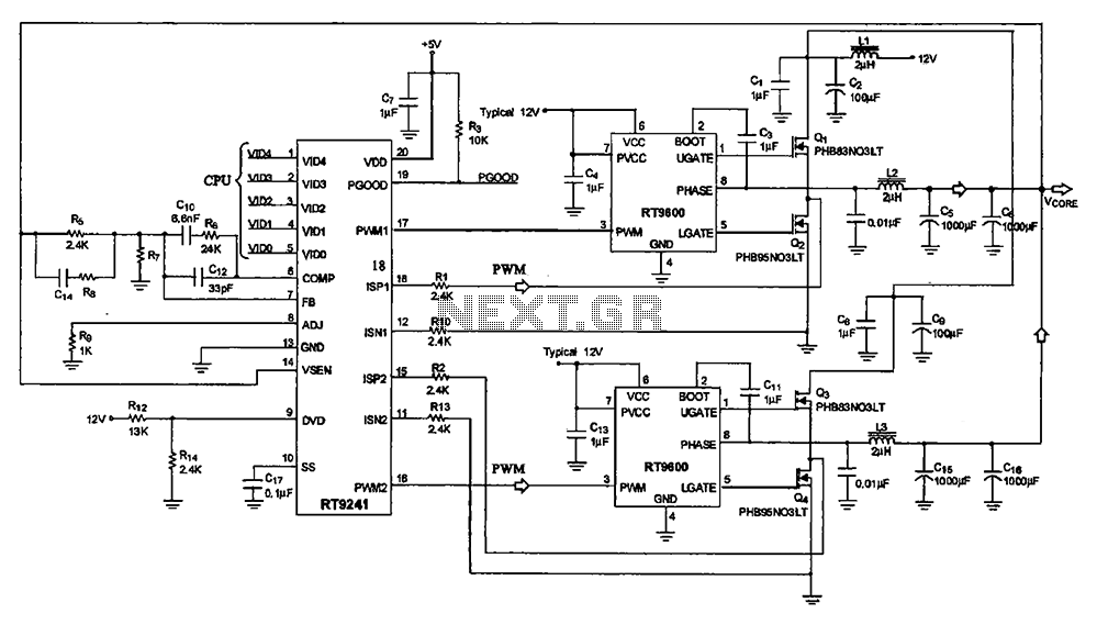
A typical computer motherboard CPU power supply circuit is primarily composed of the main power supply management chip RT9241 and additional components from the power management chip RT9600. The voltage command signal from the CPU is input into the...
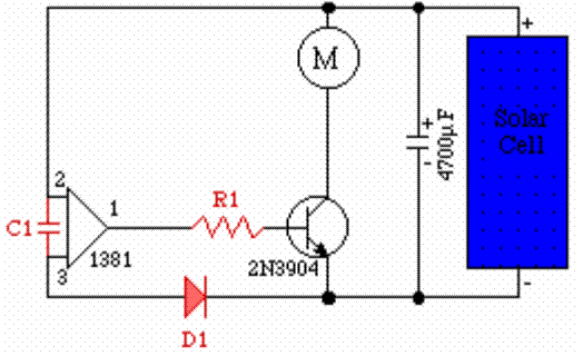
One 1381 part (CMOS voltage-controlled trigger available at different limits) should be selected to match the voltage across the motor (2V in this case). The other terminal of the motor is connected to a 3300µF capacitor, which is in...
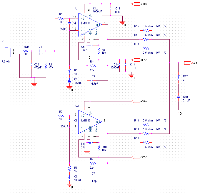
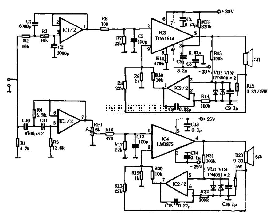
This audio amplifier design utilizes two LM3886 chips per channel in a parallel configuration, based on the PA100 parallel amplifier detailed in National Semiconductor's application note AN1192. The amplifier can deliver approximately 50W into an 8-ohm speaker and 100W...
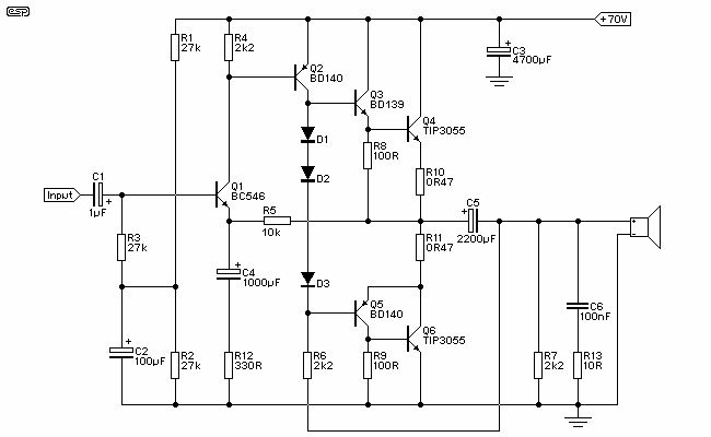
Figure 1 shows the circuit. A major change from all of the designs from that era is the speaker coupling capacitor - 1000uF (for a -3dB of 20Hz and a 8 Ohm load) was the most common value. This is...
The mechanical and electrical schematic in Figure 5 illustrates a simple circuit comprising several components. The first component is an electronic crossover section utilizing the NE5532 operational amplifier, which is known as the "Emperor of the op-amp." This section...