
smps circuit diagram

Switched-Mode Power Supplies (SMPS) are crucial in modern electronic devices due to their efficiency and compact design. An SMPS converts electrical power efficiently by switching the input voltage on and off rapidly, which reduces energy loss and heat generation compared to traditional linear power supplies.
The basic components of an SMPS circuit include a transformer, switching device (usually a MOSFET), diode, and filter capacitors. The circuit typically operates in one of several modes, such as buck (step-down), boost (step-up), or buck-boost, depending on the desired output voltage relative to the input voltage.
In a typical SMPS circuit diagram, the input voltage is first rectified and filtered to provide a stable DC voltage. The switching device is then controlled by a pulse-width modulation (PWM) signal, which adjusts the duty cycle to regulate the output voltage. The transformer is used to isolate the input from the output and can also step up or step down the voltage as required. The output is rectified and filtered to provide a smooth DC voltage to the load.
Safety features are also integral to SMPS designs, including over-voltage protection, over-current protection, and thermal shutdown mechanisms to prevent damage to the circuit and connected devices. Understanding the schematic and operation of an SMPS is essential for engineers and technicians working in electronics, as it is a fundamental component in power management for various applications, including computers, televisions, and industrial equipment.Welcome to my small blog, This blog explains a few things about smps circuit diagram, and if you`re interested, then this is worth reading, because.. 🔗 External reference
Related Circuits
Many applications require low-frequency signal generators that can deliver high-performance, high-resolution signals. This design idea presents a circuit that generates frequencies from 0 to 1 MHz, providing sinusoidal, triangular, and square-wave outputs with frequency resolution better than 0. A...
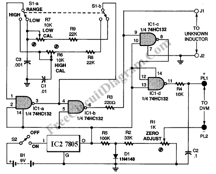
This inductance meter serves as an adapter for a digital voltmeter (DVM), enabling the voltmeter to measure the value of inductors. The inductance meter is particularly useful in designing switch mode power supplies, as it often requires hand-winding coils...
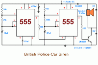
The 555 timer on the right is configured as an alarm sound generator, while the second 555 timer on the left operates as a 1 Hz astable multivibrator. The output from the left timer modulates the frequency of the...
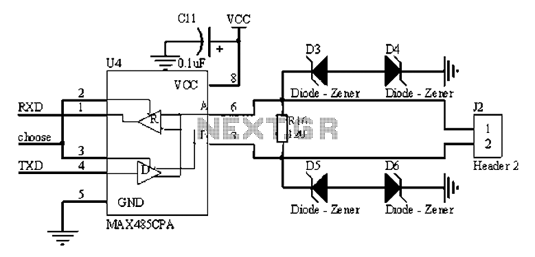
The RS485 bus is a widely used serial bus standard that employs balanced differential transmission and reception techniques, enabling it to effectively suppress common mode interference. It is particularly advantageous for communication distances ranging from tens of meters to...

This circuit switch slowly on and off the internal lights in a car. The delaying time can be adjusted changing the values of the 10k, 4M7 resistors and capacitor. More: The BUZ74 can handle voltages of 500V, but you...

CXA1019 is a high-performance, high-sensitivity FM/AM radio special manifold developed by Sony, Japan. The CXA1019 features high integration, which includes an FM/AM tuner circuit, a mixer circuit, a mute circuit, an amplifier circuit (power output of 0.5 to 1W),...