
Soft Start For Switching Power Supply
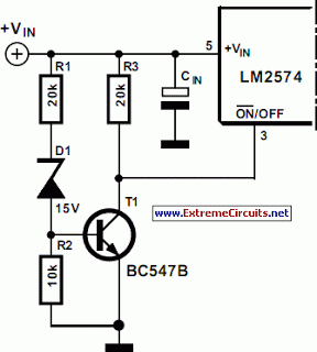
The switching power supply circuit is designed to convert a higher input voltage (24 V) into a stable lower output voltage (5 V). The circuit incorporates a regulator that is sensitive to the input voltage levels, particularly at startup. The key to ensuring reliable operation lies in managing the inrush current when the circuit is powered on. To prevent damage to the power supply or the circuit itself, a mechanism is implemented to disable the regulator until the input capacitor is sufficiently charged.
Upon powering the circuit, the input capacitor begins to charge. The zener diode, rated at 15 V, serves to clamp the voltage and protect the circuit from excessive voltage levels. The circuit is designed so that when the voltage across the capacitor reaches around 17 V, the transistor T1 is activated. This action enables the regulator, allowing it to begin supplying the desired output voltage of 5 V. The inclusion of a series resistor (22 kΩ) allows for the application of higher TTL signal voltages to control the base of the transistor, enabling flexibility in the control signal used to switch the regulator on or off.
The overall design ensures that the power supply operates efficiently while preventing overload conditions. This approach not only enhances the reliability of the circuit but also safeguards against potential failures due to excessive input current at startup. The integration of an on/off switch within the regulator simplifies the control mechanism and provides an effective solution for managing the power supply's operational states.Switching power supply whose output voltage is appreciably lower than its input voltage has an interesting property: the current drawn by it is smaller than its output current. However, the input power (UI) is, of course, greater than the output power. There is another aspect that needs to be watched: when the input voltage at switch-on is too low , the regulator will tend to draw the full current. When the supply cannot cope with this, it fails or the fuse blows. It is, therefore, advisable to disable the regulator at switch-on (via the on/off input). until the relevant capacitor has been charged. When the regulator then starts to draw current, the charging current has already dropped to a level which does not overload the voltage source. The circuit in the diagram provides an output voltage of 5 V and is supplied by a 24 V source. The regulator need not be disabled until the capacitor is fully charged: when the potential across the capacitor has reached a level of half or more of the input voltage, all is well.
This is why the zener diode in the diagram is rated at 15 V. Many regulators produced by National Semiconductor have an integral on/off switch, and this is used in the present circuit. The input is intended for TTL signals, and usually consists of a transistor whose base is accessible externally.
This means that a higher switching voltage may be applied via a series resistor: the value of this in the present circuit is 22 k. When the voltage across the capacitor reaches a level of about 17 V, transistor T1 comes on, whereupon the regulator is enabled.
🔗 External reference
Related Circuits
The voltage regulator integrated into the Arduino Uno is a linear-type regulator, which exhibits poor efficiency. When operating the ATmega238 at 5V with a 9V battery, nearly half of the battery's energy is wasted as heat by the regulator....
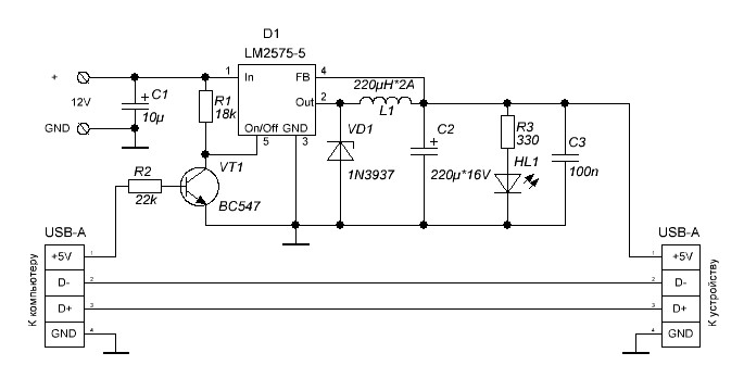
Additional power supply for USB devices. Refer to the page for an explanation of the related circuit diagram. The additional power supply for USB devices is designed to enhance the power availability for devices that may require more current than...
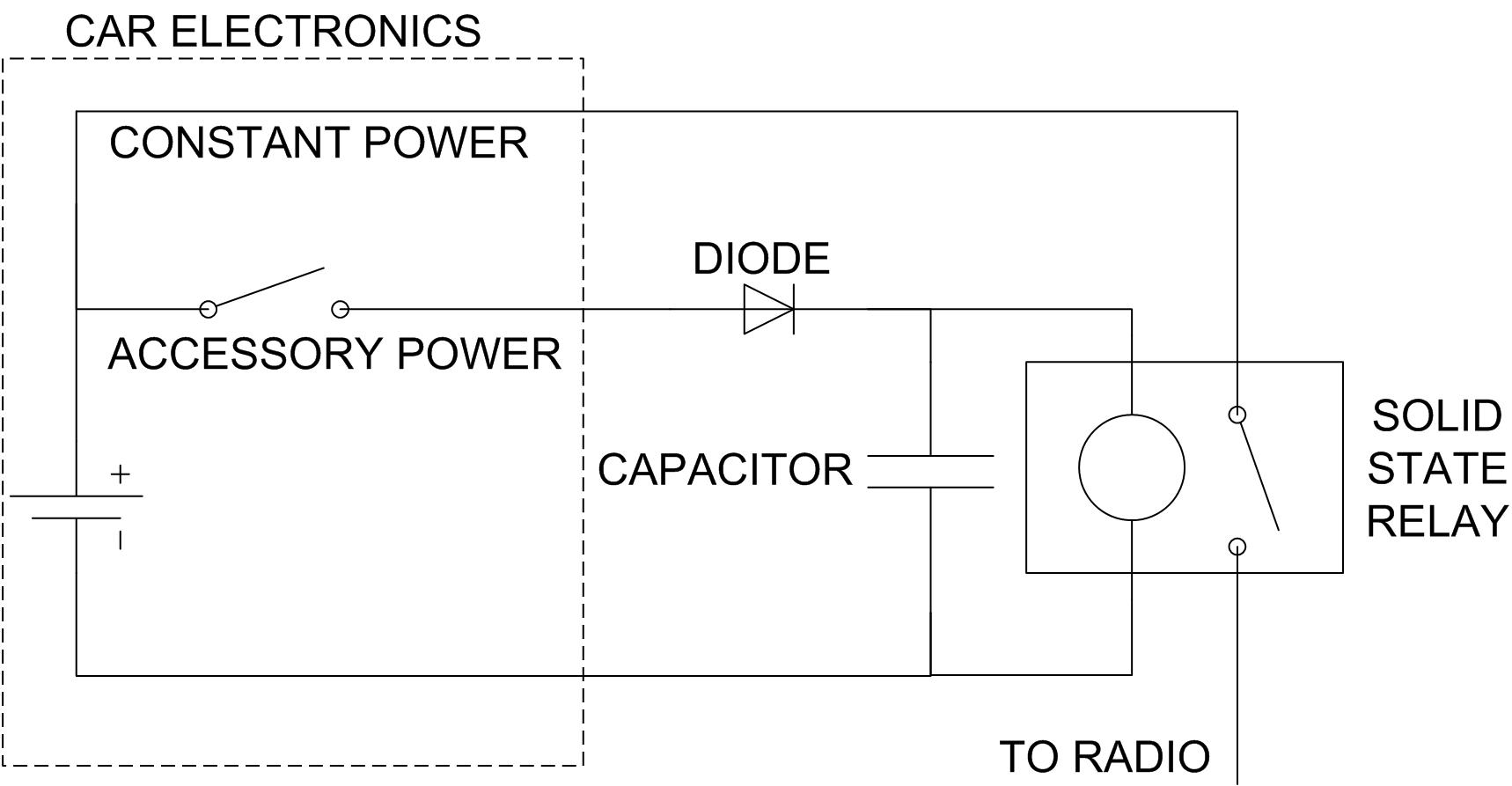
The car radio has the issue of losing track of the CD playback position when the ignition is turned off. This can be problematic during long journeys, especially when leaving an audiobook playing for passengers while refueling. A simple...
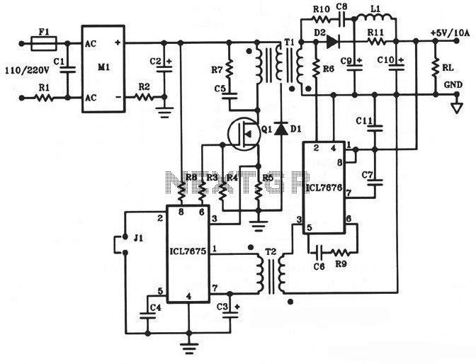
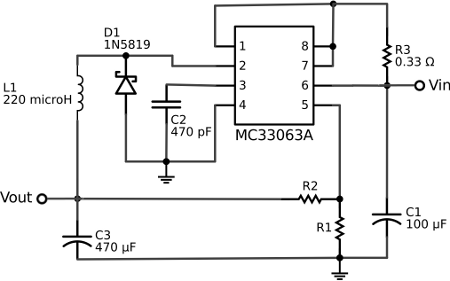
The following diagram illustrates a 50W offline switching power supply circuit design. This circuit is powered by a MOSFET, specifically the BUZ80A/IXTP4N8 for a 220V AC voltage input and the GE IRF823 for a 110V AC voltage input. The...
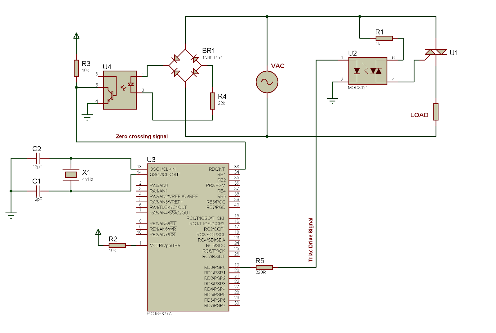
The image above clearly demonstrates phase angle control, where the output voltage is regulated by the gate drive signal applied to a thyristor. Phase angle control is a technique of pulse width modulation (PWM) used with alternating current (AC)...
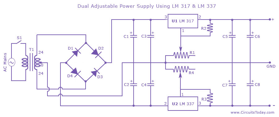
Dual adjustable power supply circuit with a diagram using IC LM317 and LM337. This variable power supply circuit has a range of 1.2 volts to 30 volts. The dual adjustable power supply circuit utilizes the LM317 and LM337 voltage regulators...