
Soft Start For Switching Power Supply
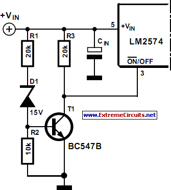
The switching power supply circuit functions by converting a higher input voltage (24 V) to a stable lower output voltage (5 V) while maintaining efficiency through controlled current draw. The process begins when the circuit is powered on; initially, the regulator is disabled to prevent excessive current draw that could damage the supply or blow fuses. The capacitor in the circuit plays a critical role in this process. It charges up to a sufficient voltage level, specifically around half of the input voltage (12 V), ensuring that when the regulator is enabled, it operates within safe limits.
The zener diode rated at 15 V serves as a voltage reference and protection mechanism in the circuit. It ensures that the voltage across the capacitor does not exceed its rated value, thus preventing damage to the components. When the voltage reaches approximately 17 V, transistor T1 is turned on, which in turn activates the regulator. This allows for the stable output voltage of 5 V to be supplied to the load.
The circuit design incorporates a TTL-compatible input for the on/off control, which is essential for interfacing with digital logic circuits. The use of a series resistor (22 k) with the base of the transistor allows for flexibility in switching voltage levels, accommodating various control signals without risking damage to the transistor. Overall, this design ensures reliable operation of the switching power supply while protecting against potential overcurrent situations during start-up.Switching power supply whose output voltage is appreciably lower than its input voltage has an interesting property: the current drawn by it is smaller than its output current. However, the input power (UI) is, of course, greater than the output power. There is another aspect that needs to be watched: when the input voltage at switch-on is too low , the regulator will tend to draw the full current. When the supply cannot cope with this, it fails or the fuse blows. It is, therefore, advisable to disable the regulator at switch-on (via the on/off input). until the relevant capacitor has been charged. When the regulator then starts to draw current, the charging current has already dropped to a level which does not overload the voltage source. The circuit in the diagram provides an output voltage of 5 V and is supplied by a 24 V source. The regulator need not be disabled until the capacitor is fully charged: when the potential across the capacitor has reached a level of half or more of the input voltage, all is well.
This is why the zener diode in the diagram is rated at 15 V. Many regulators produced by National Semiconductor have an integral on/off switch, and this is used in the present circuit. The input is intended for TTL signals, and usually consists of a transistor whose base is accessible externally.
This means that a higher switching voltage may be applied via a series resistor: the value of this in the present circuit is 22 k. When the voltage across the capacitor reaches a level of about 17 V, transistor T1 comes on, whereupon the regulator is enabled.
🔗 External reference
Related Circuits
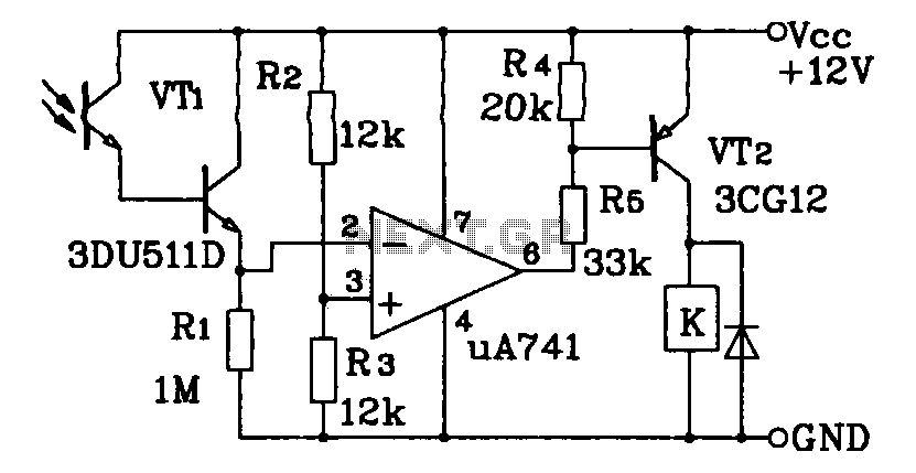
This circuit application utilizes a Darlington phototransistor for light-triggered switching. The design incorporates a Darlington phototransistor and an operational amplifier (op-amp), allowing the circuit to respond to very faint light levels. The circuit can be modified to trigger in...
One very important part of a tube amplifier is the power supply. It is crucial for the quality of the whole system. Especially beginners encounter problems like hum or drift that can become quite annoying. But rescue is ahead:...
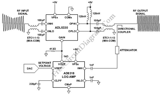
This is a circuit for Closed-Loop Automatic Power Control for RF Applications. The circuit utilizes a log detector (AD8318) and a variable gain amplifier (VGA) (ADL5330). The Closed-Loop Automatic Power Control (APC) circuit is designed to maintain a consistent output...
In the absence of radiation, no current is drawn. At normal background radiation levels, the power consumption is extremely low. The instrument may be left on for several months without changing batteries. In this way, the detector is always...
The air-cored inductor L1 is constructed using 13 turns of 1mm diameter enamelled copper wire, featuring an inner diameter of 10mm. The completed inductor is positioned over R7, with its terminals soldered to those of the resistor. All electrolytic...
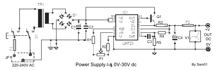
This is a simple regulated power supply circuit based on the well-known LM723 voltage regulator, which drives a transistor Q1 (2N3055). The output voltage regulation is achieved using potentiometer R1, allowing for an adjustable range from 0V to approximately...