
Solenoid Driving Circuit
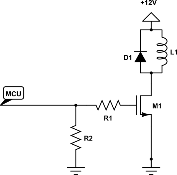
The solenoid's operation hinges on the precise management of current flow, necessitating a robust circuit design that incorporates both the solenoid's characteristics and the MOSFET's electrical parameters. The solenoid's inductive nature requires careful consideration of current limitations to prevent damage to components. The integration of a bypass capacitor is crucial, as it provides a smoothing effect for high-frequency transients, thereby protecting circuit integrity.
The choice of a MOSFET with a high breakdown voltage ensures that the circuit can handle unexpected voltage spikes without failure. The on-state resistance (R_dson) of the MOSFET, while contributing to a minor reduction in current, also plays a role in heat generation and efficiency. In this design, the power dissipation resulting from the R_dson is minimal, which is advantageous for maintaining the overall thermal performance of the circuit.
The gate drive voltage is another critical parameter, as it directly influences the MOSFET's switching behavior. Operating within the specified voltage range ensures optimal performance, but the potential for operation in linear mode due to lower gate voltages must be addressed. This condition can lead to increased power loss and reduced efficiency, making the selection of appropriate gate drive circuitry essential.
To optimize the switching performance, a PWM gate driver capable of delivering sufficient peak current is recommended. The use of a 10 Ohm gate resistor aids in rapid gate charging, thus reducing the duration of linear operation and enhancing switching efficiency. The relationship between the gate voltage, drain current, and drain-source voltage, as illustrated in the datasheet, should be referenced to ensure that the MOSFET operates within its intended parameters.
In conclusion, the design of the solenoid-driven circuit requires a comprehensive understanding of the interplay between the solenoid's inductive properties, the MOSFET's electrical characteristics, and the overall circuit dynamics. Careful selection of components, particularly in terms of voltage ratings and resistances, along with appropriate gate drive strategies, will contribute to a reliable and efficient design.The solenoid requires a certain amount of current to generate its magnetic field. If the solenoid was a perfect inductor, the DC current would rise above all means and would most likely damage other circuit components. However, solenoids inherently have a significant amount of DC resistance used to limit the current magnitude.
Provided you place a bypass capacitor (to absorb high-frequency current pulses induced by changing the current magnitude) between GND (close to the mosfet source) and the 12 V connection solenoid, you do not have to worry about a significant overshoot. Your selected mosfet has breakdown voltage of 100 V, which is certainly an overkill. The mosfet also has a non-zero on-state resistance Rdson (160 mOhm), which will slightly reduce the current through the solenoid.
Another implication of Rds is mosfet power dissipation - which is negligible in this case (160 mOhms provided the channel is fully open). 2) One problem I see with your circuit is that the gate voltage will be 3. 3 V but the MOSFETs gate voltage is specified between 2 and 4 V. In practice, it`s fine because even if you get a "bad" part, the MOSFET will still partially close and allow current current to flow through its channel.
An implication of low gate voltage is that the switch will work in the linear mode, where its on-state resistance is much higher than the guaranteed value. EDIT The gate threshold voltage is the minimum voltage where the MOSFET starts conducting current; however, the channel current would most likely not be enough to turn on the solenoid.
Look at Figure 1 in datasheet, which correlates gate voltage with drain current and drain-source voltage. allowed source peak current - some PWM gate drivers can well support 30 A peak, which (with 10 Ohm gate resistor - R1) very quickly charges the gate and thus minimizes time spent in the linear mode.
I assume you drive the gate from an MCU pin - look at the datasheet on allowed pin current. That current is, however, the average current so you can drive much more on a peak basis. I would guess that 50 mA is fine -> 3. 3V / 50 mA ~= 70 Ohms would be a good value for this application. 🔗 External reference
Related Circuits
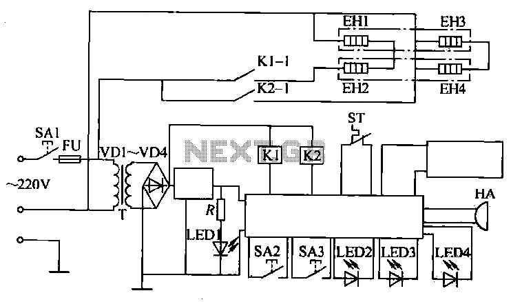
The circuit operates by activating switch SA1, which powers a 220V transformer that converts AC voltage to DC through a bridge rectifier, supplying power to the computer control panel. The temperature for cooking food is set on this control...
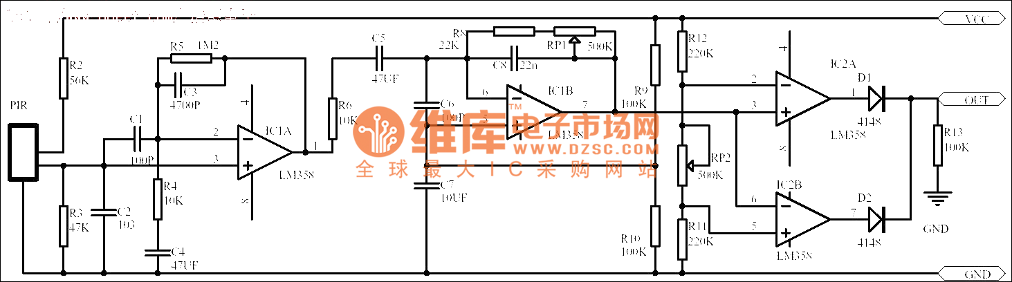
Passive human body infrared sensor circuits are generally similar in design, although some may have fewer stages. The circuit illustrated is sourced from the NICERA manufacturer and is considered a classic example. The front-end stage consists of a low-frequency...
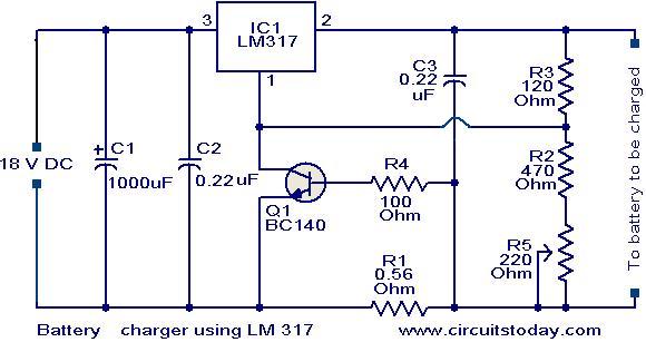
This is a simple yet effective battery charger circuit utilizing the LM317 integrated circuit (IC). The circuit is designed for charging 12V lead-acid batteries and can be easily assembled on a general-purpose printed circuit board (PCB). The core component...
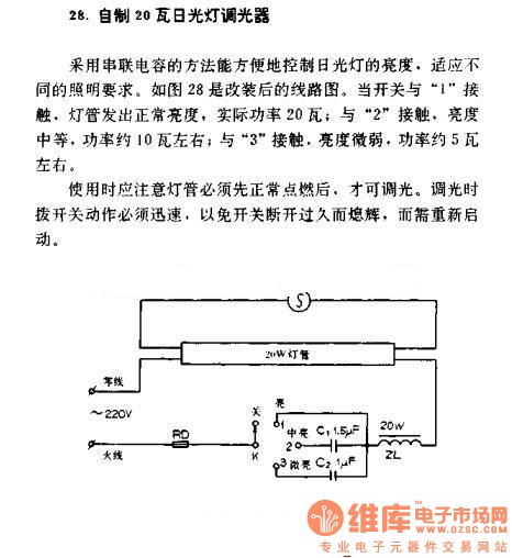
A homemade 20W fluorescent lamp dimmer utilizes a series capacitor connection to effectively control the brightness of fluorescent lamps, allowing for adaptability to various lighting requirements. In the modified circuit diagram (Figure 28), when the switch is set to...
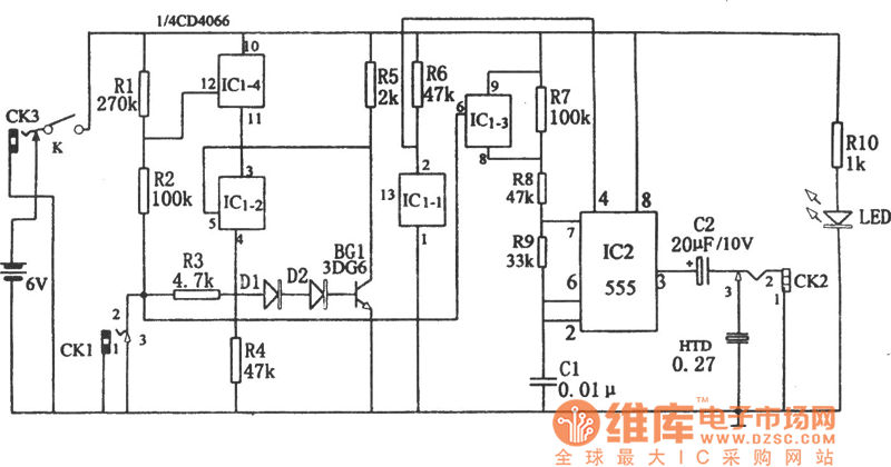
The circuit diagram illustrates a five-use tri-state audio logic pen utilizing components such as the CD4066 and a 555 timer. The primary elements include a multivibrator, a four-way switch (CD4066, designated as IC1), and a gate circuit formed by...
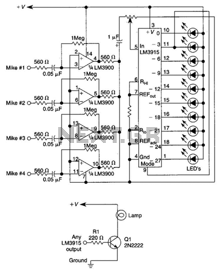
This circuit will produce an output when the sound exceeds a preset level. The LM3915 is a log-output bar graph driver. A transistor driver is used for higher current loads. To drive heavy-current loads with an LM3915 output, a...
Warning: include(partials/cookie-banner.php): Failed to open stream: Permission denied in /var/www/html/nextgr/view-circuit.php on line 713
Warning: include(): Failed opening 'partials/cookie-banner.php' for inclusion (include_path='.:/usr/share/php') in /var/www/html/nextgr/view-circuit.php on line 713