
Solid State Circuits 2
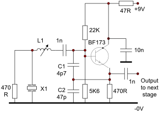
This oscillator circuit is designed to utilize a crystal for frequency stabilization, enabling precise frequency generation suitable for various RF applications. The configuration employs a Colpitts oscillator topology, which is known for its stability and simplicity. The circuit's performance is contingent on careful selection of components, particularly the resonant inductor and capacitors, which must be matched to the intended frequency of operation. The use of a buffer stage is critical in maintaining signal integrity, especially in applications where the oscillator output needs to drive multiple loads or stages.
In practice, the choice of transistors is also essential, as their frequency response characteristics can significantly influence the overall performance of the oscillator. The output waveform's non-sinusoidal nature may necessitate additional filtering or shaping if a clean sine wave is required for subsequent stages. The incorporation of a resistor across the crystal serves a dual purpose: it stabilizes the oscillation frequency and prevents unwanted resonances that could lead to circuit instability.
Overall, this circuit exemplifies a robust solution for generating RF signals across a wide frequency range, with careful attention to component selection and circuit layout ensuring optimal performance in practical applications.This circuit can be used from low frequencies to at least 120MHz using series resonant crystals on their fundamental or overtone mode. The output can be taken from the feedback tap as shown, a low impedance winding on L2 or from the drain of the J310 via a low value capacitor.
The following stage should be used a a buffer to isolate subsequent sta ges from the oscillator. The combined series value of C1 and C2 resonates with inductor L1 at the desired frequency and crystal X1 must have a fundamental or overtone series resonance as appropriate at the same frequency. C2 is about five times the value of C1 Inductor L2 is generally only required at frequencies above about 60MHz and must be chosen to resonate with the total parallel capacitance of X1 at the frequency of oscillation.
If the circuit shows signs of free running oscillation controlled by L1 then L2 will be required. The parallel capacitance of X1 will typically be 4 - This circuit is primarily intended for use as an overtone oscillator and will work from 20MHz to 120Mhz depending on the crystal and active device. Operation is extremely stable but the output level is fairly low - pk. L1, C1/C2 and the input capacitance of the transistor act as a quarter wave network, converting the low impedance series resonance of the crystal into a high impedance parallel resonance at the base of the transistor.
C1 may not be needed at higher frequencies depending on the internal base/emitter capacitance. This circuit is a Colpitts fundamental mode parallel resonant oscillator for crystals designed for use with a 30pF load capacitance. Values shown are suitable for 8 - 12Mhz and will require changing for significantly different frequencies.
Transistors TR1 and TR2 should be characterised for the required frequency range. Devices like the BC108 have been shown to work in this circuit but are not specified at high frequencies. Preferred devices would be BF115, BF199 etc. The RF output is not sinusoidal. The 470R resistor across the crystal suppresses oscillation at the parallel resonant frequency and must not be omitted.
Most RF characterised transistors will work in this circuit. This fundamental mode Pierce oscillator can be used over a wide frequency range with little or no changes to component values. The circuit to the right was originally developed by myself in the 1970s using a 2N5245 RF JFET which had a relatively low Idss range but they are now very difficult to obtain.
A J310 has been used instead which has an Idss range of 24 - Although the higher value drain resistor gives more gain at the low frequencies, there is an obvious reduction in output level at the higher frequency end due to the RC time constant impacting on circuit gain and slew rate. As with most oscillators the output power level is low. If it needs to be distributed around a number of circuits then an emitter follower or equivalent buffer stage should be included.
A bipolar npn emitter follower may be DC coupled to the FET drain via a 47ohm resistor to suppress any tendency to oscillate at VHF. If you decide to replace the drain resistor with an RF choke then the emitter follower should not be DC coupled to the drain as the drain voltage will exceed the supply line on positive half cycles.
🔗 External reference
Related Circuits
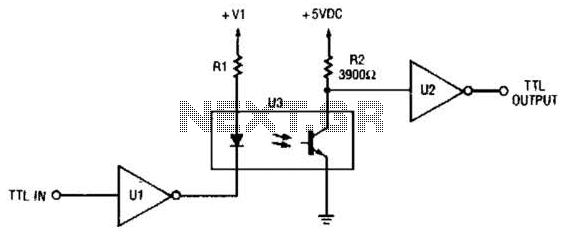
This circuit is a TTL-to-TTL isolator circuit. The driver circuit is an open-collector TTL inverter (U1). When the input is high, the output of the inverter is low. Thus, when the input is high, the output of U1 grounds...
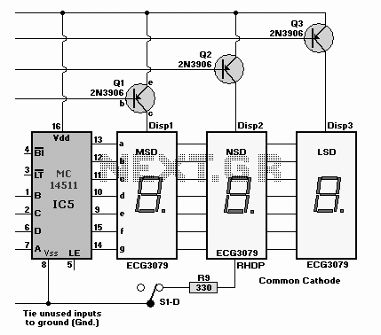
A brief history: Like many tutorials, this one begins with a historical overview. However, it must be noted that there is limited background information available regarding the development of 7-segment displays. 7-segment displays are widely used electronic components that...
This circuit is designed to drive a relay coil using a low power output, typically from an integrated circuit (IC) such as a 555 timer or a TTL/CMOS device. It facilitates the switching of high loads or loads requiring...
The circuits in Figure 1 and Figure 2 demonstrate specific advantages over the circuit presented in the Design Idea in EDN, titled "Circuit detects first event," published on May 3, 2001, page 89. The n-player first-event detection circuit provides...
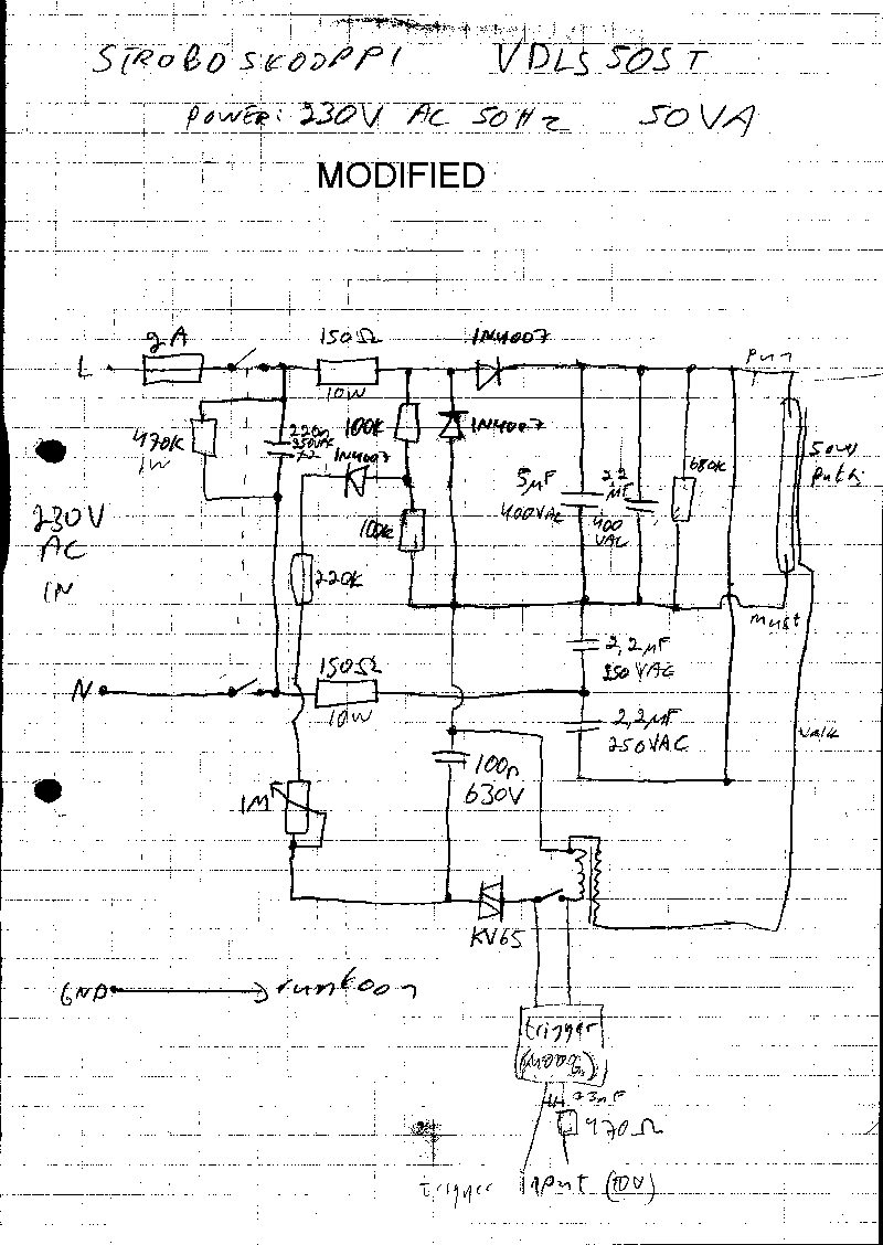
This page provides information on circuits that can trigger stroboscopes from external circuits. The circuits are designed to be integrated into stroboscope systems, allowing them to be activated using an external trigger pulse. The standard trigger pulse utilized in...
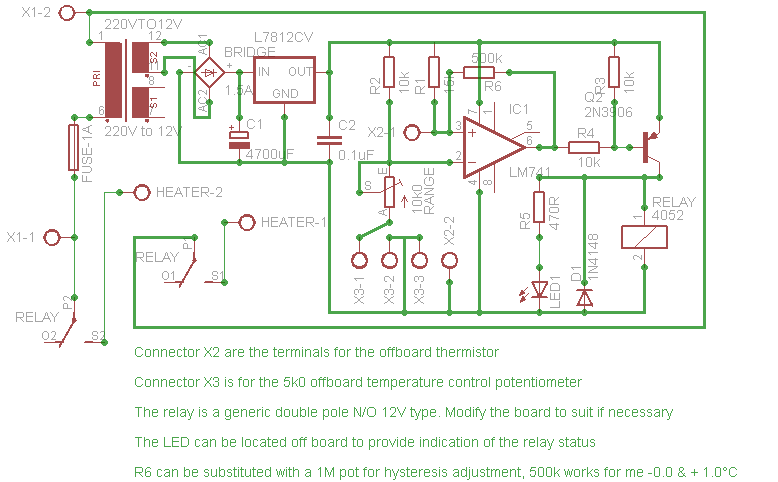
Affordable, straightforward, and precise thermostat circuits with instructions. The thermostat circuit is designed to provide a cost-effective and reliable solution for temperature control applications. It typically utilizes a temperature sensor, such as a thermistor or a thermocouple, to monitor the...