
Solid-State Relay
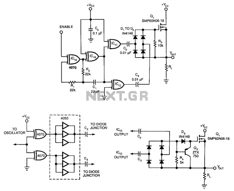
The described circuit employs a power MOSFET in conjunction with a quad exclusive-OR oscillator to function as a solid-state relay, effectively managing high-speed switching applications. The gated oscillator, comprising IC1A and IC1B, is configured to operate at a frequency of 500 kHz. The components R1, R2, and C1 are pivotal in establishing this frequency, ensuring that the oscillator maintains its operational integrity.
The diode bridge formed by diodes D1 through D4 plays a crucial role in rectifying the AC signal produced by the oscillator, allowing for the conversion of this signal into a usable DC voltage. This rectified voltage is then used to charge capacitors C2 and C3, which are integral for providing the necessary gate drive voltage to the n-channel MOSFET.
The function of resistor R3 is critical for controlling the turn-off characteristics of the MOSFET. By discharging the gate charge quickly when the oscillator is disabled, R3 ensures that the MOSFET turns off efficiently. The selection of a 10 kΩ resistor is significant as it achieves a turn-off time of 800 ns while maintaining the integrity of the gate's enhancement voltage.
For applications requiring even faster turn-off times, the circuit can be modified by introducing a PNP transistor configured as a diode-steering emitter-follower. This modification allows for a further reduction of the turn-off time to 100 ns, enhancing the overall performance of the relay.
Incorporating a hex buffer into the circuit design can also improve the output drive capability, ensuring that the complementary outputs can effectively handle larger loads without compromising performance. This enhancement is particularly beneficial in applications where multiple outputs are required to drive larger capacitive or inductive loads. Overall, the combination of these components creates a robust and efficient solid-state relay suitable for a range of electronic applications. A power MOSFET and a quad exclusive-OR oscillator makes an effective solid-state relay. Figure 75-5(a)"s capacitively iso lated drive circuit provides gate drive to turn on the n-channel device. This consists of a gated oscillator (IC1A and IC1B running at 500 kHz, set by Rl, R2, and CI). The diode bridge (Dl through D4) rectifies the charge transferred through C2 and C3. When you disable the oscillator, R3 discharges the stored gate charge, thereby turning off the MOSFET. R3 needs to allow fast turn-off times without loading the gate"s enhancement voltage. A value of 10-KOhmhm is sufficient to produce a turn-off time of 800 with an 18-mQ SMP60N06-18 MOSFET.
The measured turn-on time is 150 . You can reduce the turn-off time to 100 by using a pnp transistor as a diode-steering emitter-follower in the MOSFET gate circuit (Fig. 75-5(b)). Adding a hex buffer to Fig. 75-5A"s circuit increases the drive capability of the complementary outputs. 🔗 External reference
Related Circuits

This circuit is similar to the one above, but uses a N channel mosfet such as IRF530, 540, 640, etc. in place of the NPN transistor. Smaller mosfets could be used, but I don't know the part numbers. I...
A circuit that activates a relay upon detecting audio pulses from one channel of an MP3 player. The intention is to synchronize recorded audio pulses with music to control a motor for mouth movement. For a stereo player, music...
The figure below illustrates the use of a relay in the starting circuit. The power input connects through a resistor R, which serves two purposes: first, it prevents a large current from the capacitor C1 from affecting the power...
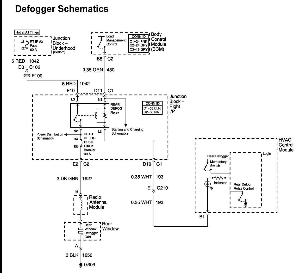
A 2004 Chevrolet Impala is experiencing issues with the rear defogger. The owner is unable to locate the fuse for the rear defogger, although the relay has been found. Both the manual and the vehicle's diagram indicate a 30-amp...
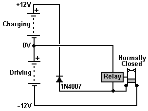
This document explains the adaptation of a standard 40 amp car relay, converting it from a "normally open" contact configuration to a "normally closed" contact configuration. While it is possible to perform this modification, automotive relays with "normally closed"...
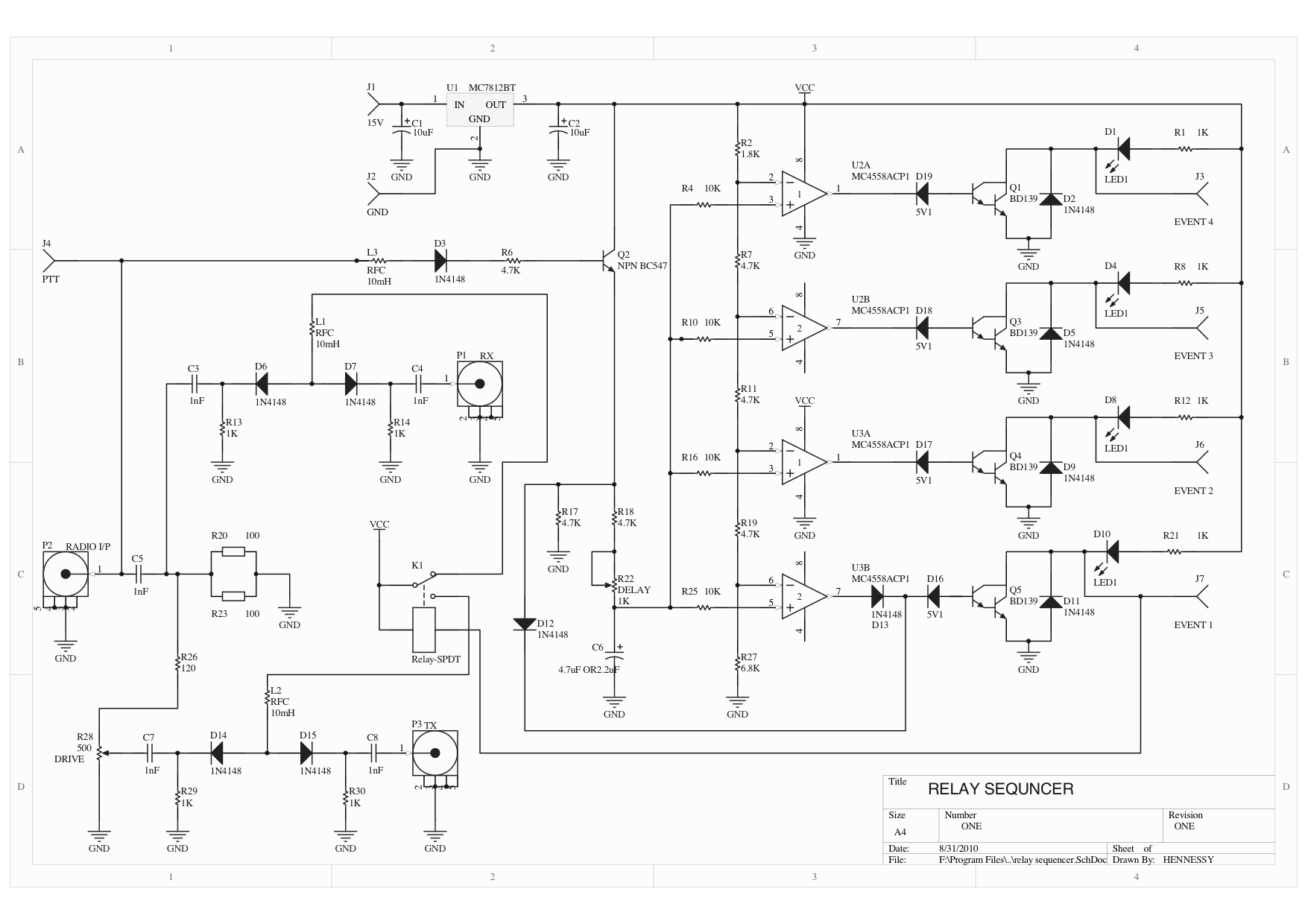
A relay sequencer is utilized in a radio transverter to activate specific stages sequentially after a brief delay. This project outlines the construction of this sequencer, which features a stage that switches the output/input of the driving radio to...