
Relay Sequencer Board
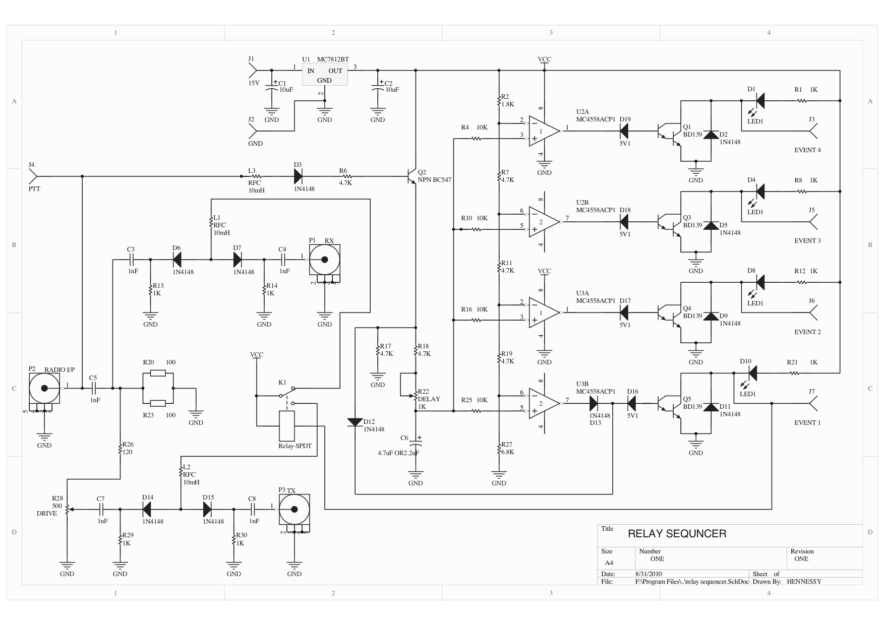
The relay sequencer circuit is designed to manage the switching between the RX and TX paths in a radio transverter, facilitating smooth transitions between receiving and transmitting modes. The circuit employs a relay, which is controlled by the state of the transverter, ensuring that the correct signal path is selected based on operational needs. The use of K1 in both NC and N/O positions allows for seamless switching without interruption in signal flow.
The timing mechanism is critical in this design, as it employs a capacitor, C6, to create a delay before activating the output transistors. This delay is adjustable, providing flexibility in tuning the response of the sequencer to suit different operational requirements or preferences. The charging and discharging behavior of C6, governed by the resistors R18 and R22, determines the timing of the sequencer's operation. The calculated time constant ensures that the outputs are activated in a controlled manner, preventing simultaneous activation that could lead to signal distortion or interference.
The op-amps serve a dual purpose: they provide voltage thresholds for the sequencing and also drive the output transistors. By operating in sink mode, the transistors can handle higher voltages and currents, ensuring that the system can manage the power levels typically encountered in radio frequency applications. The inclusion of LEDs provides visual feedback, indicating the status of each output, which is essential for troubleshooting and operational awareness.
This relay sequencer circuit is thus a vital component in radio transverter applications, ensuring reliable and efficient operation while maintaining signal integrity during transitions between receiving and transmitting states.A relay sequencer is used in a radio transverter and is use to activate particular stages in order after short delay. This project describes how to build this sequencer. It has the following features. This stage is used to switch the output / input of the driving radio to the corresponding RX IF output or the TX IF input depending the current stat
e of the relay sequencer. When the sequencer is not activated (The radio is receiving) K1 is in its NC position, suppling DC voltage to L1 forward biasing D6, D7 and then flowing through R13 and R14 (As shown in blue arrows). C3 and C4 are used to block the DC. Once D6, D7 are conducting the RF signal is able to pass from the RX IF port to the radio input / output port (As shown in red).
When the sequencer is activated (The radio is transmitting) K1 is in its N/O position suppling DC voltage to L2 forward biasing D14, D15 and then flowing through R29 and R30. Once D14, D15 are conducting the RF signal is able to pass from the radio output port to the TX IF port (As shown in green).
The second half of the circuit is the relay sequencer. Once activated the four output transistors will start to turn on in order after a short adjustable delay. The circuit in used the set up below. The circuit works by using the time it take C6 to charge up and the time it takes to discharge. As the circuit is activated the voltage across C6 increases over time as shown below. The capacitor takes 5 time consents to change up to full. 1T = R * C (C6* R18+R22). The 4 op-amps are setup to turn on at different voltages as C6 charges up. The op-amps are used to drive four transistors in sink mode so a higher switching voltage can be used.
The transistors are able sink a MAX 1. 5A at 80V and four LEDs are used for indication of the outputs are active. 🔗 External reference
Related Circuits
This is a practical expansion board designed for a PIC development board, intended for DIY use with a 16x2 alphanumeric LCD. The expansion board connects to the PIC development board, providing LCD support, which is essential for numerous projects...
This circuit design for a low current relay is intended for use in battery-operated electronic devices, with an operating current in microamperes (µA). It utilizes a bistable relay and additional components to enable the relay to function similarly to...
While the battery is charging, its voltage is measured at V. If the measured voltage is lower than the minimum threshold, the relay will be activated, connecting the charger circuit. When the battery voltage exceeds the maximum set point,...
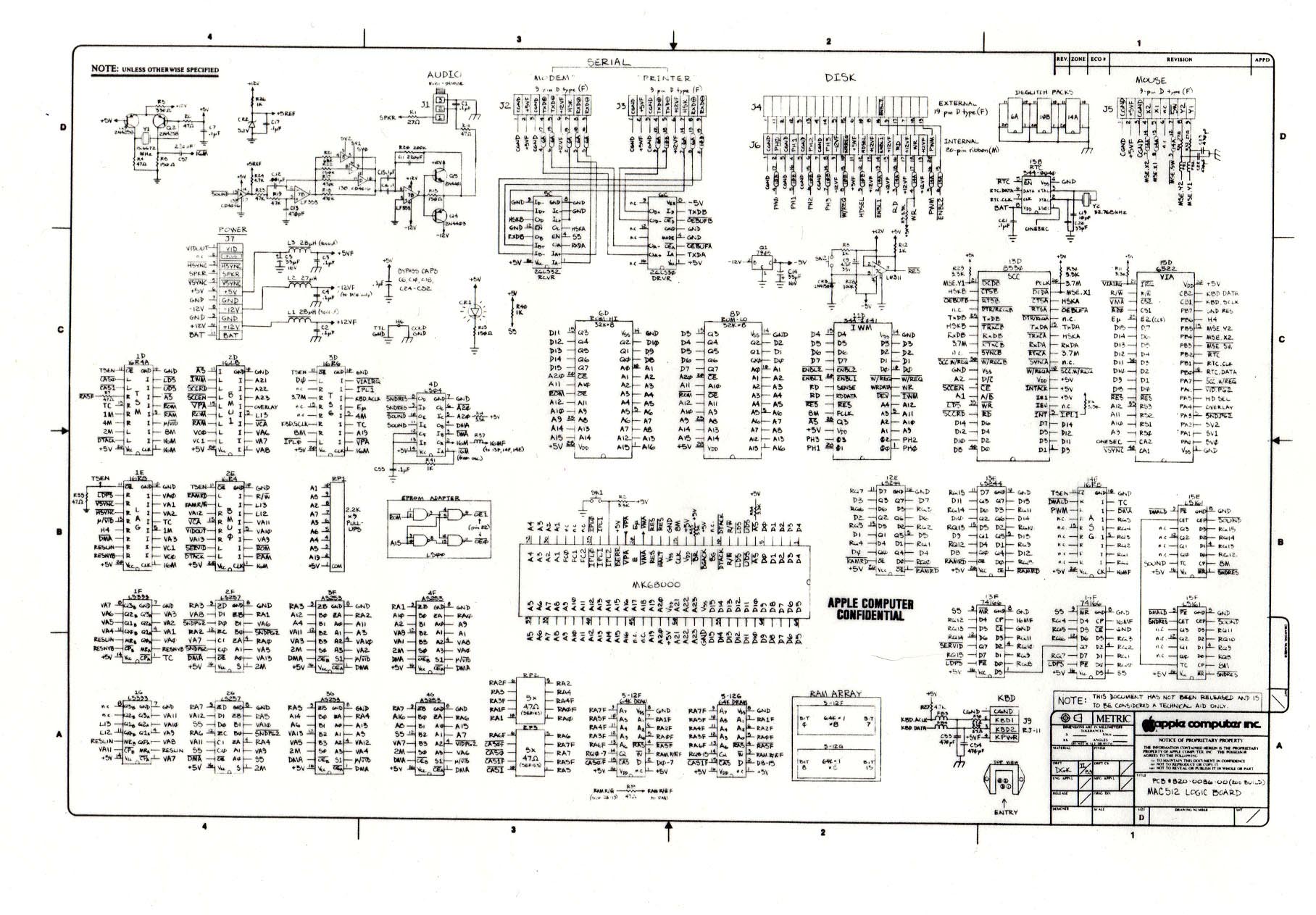
The following is one of the rare and significant documents at DigiBarn, the only known copy of the complete schematic specification for the 512K Macintosh Logic Board. Co-authored by Daniel Kottke, this design served as the foundation for the...
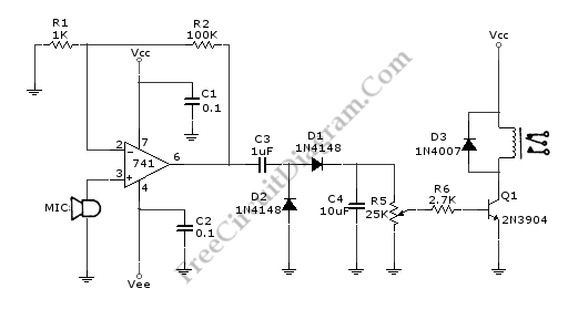
This is a relay circuit that detects the presence of sound to activate the relay. This sound-controlled relay can be utilized as a voice-operated switch or for controlling lights. The sound-activated relay circuit typically employs a microphone or a sound...
This article discusses the utilization of old PCs as simple controllers. Many obsolete systems, such as the 8088, 8086, 80286, 80386, and 80486, are no longer capable of running modern software, yet they can still function effectively. Often, individuals...