
Square transform circuit diagram
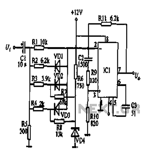
The described circuit leverages the non-linear characteristics of diodes in conjunction with an operational amplifier to achieve a square-law response to input signals. The operational amplifier serves as a high-gain amplifier, which enhances the output signal proportional to the input signal's square.
In this configuration, the resistor-diode network is pivotal. The diodes, with their varying turn-on voltages, create a scenario where different segments of the input voltage are processed differently, leading to a non-linear output. When the input voltage is low, only the diode with the lowest turn-on voltage conducts, while as the input voltage increases, additional diodes begin to conduct, effectively decreasing the overall impedance of the network.
The resistor values in the network must be chosen carefully to ensure that the desired square-law characteristics are achieved over the intended range of input voltages. This involves calculating the expected voltage drops across each diode and setting the resistor values to maintain the appropriate gain for the operational amplifier.
Furthermore, the operational amplifier should be configured in a non-inverting mode to ensure that the output voltage is always positive, which aligns with the square-law function. Feedback components may also be included to stabilize the gain and improve linearity across the input voltage range.
This square-law converter circuit finds applications in a variety of fields, including signal processing and analog computing, where it is essential to convert signals in a non-linear fashion. The design must account for temperature variations and diode characteristics to ensure consistent performance. Proper layout and component selection will enhance the reliability and accuracy of the circuit, making it suitable for precision applications. At the input of the operational amplifier plus a resistor - diode network can be constructed square-law function conversion circuit. Resistor - diode network and form a voltage divider with the input voltage changes, the partial pressure of having different coefficients. Since the three diodes (VD1 ~ VD3) have different turn-on voltage, so as the input signal increases, the overall network impedance decreases, the results of the operational amplifier gain is increased. The resistance - the relationship between input and output diode network network, with an approximate square law characteristic, therefore, the whole forming a square-law converter circuit.
Related Circuits
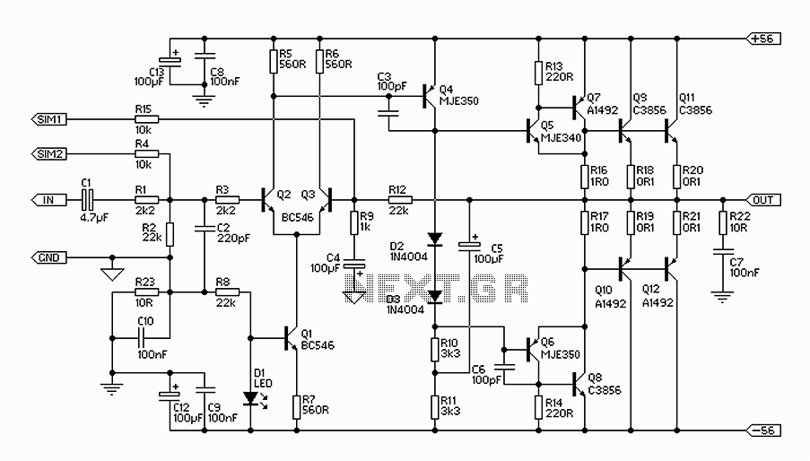
The 300W amplifier circuit presented is a conventional design. It includes connections for the internal SIM and incorporates filtering for RF protection (R1, C2). The input is facilitated through a 4.7µF bipolar capacitor, which offers substantial capacitance in a...

The resistors were not measured precisely, and given their ±5% tolerance, along with a Vref range of 1.2 to 1.3 volts, it is possible to exceed 6 volts in certain scenarios. A discussion arose regarding the effectiveness of these...
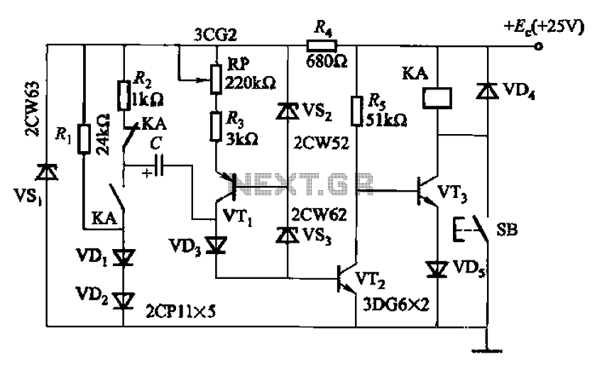
Charging time relay circuit 2 is a long delay circuit. When the capacitor C is 5000 µF, the delay can be up to 1.3 hours. Transistors VT1 and the VS2, VS3 group function as a constant current source to...
In spite of the improvement of communication link and despite all progress in advanced communication technologies, there are still very few functioning commercial wireless monitoring systems, which are most off-line, and there are still a number of issues to...
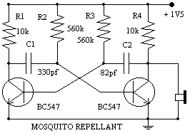
The Astable Multivibrator, which is generally used as a signal generator, is once again used here to generate the desired frequencies. It is an excellent example of the fact, how versatile simple basic electronic circuit can be. It seems...
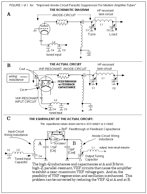
This is the unedited version of the article "Improved Anode-Circuit Parasitic-Suppression For Modern Amplifier-Tubes," which was published on page 36 of the October 1988 issue of QST. A subsequent discussion on this topic appeared in the September and October...