
SQUARE TRIANGLE VCO
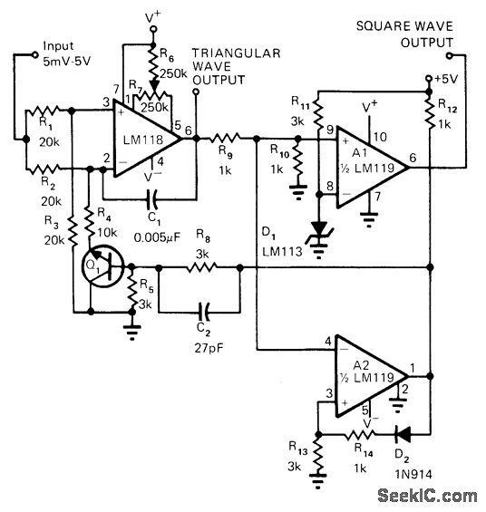
The circuit operates by employing two comparators to generate square and triangle waveforms. The control voltage applied to the circuit determines the frequency of these outputs, allowing for precise adjustments. The comparators function by comparing the input voltage to a reference voltage, which is set to define the desired output levels.
The triangle waveform is generated through a charging and discharging process, where the output rises linearly until it reaches the peak value of 2.44 V, at which point comparator A1 engages to drive the output high. As the voltage decreases to 0 V, comparator A2 activates, driving the load low. This switching mechanism ensures that the output maintains good linearity across the specified control voltage range.
The design of this circuit highlights the versatility of comparators, which can perform functions beyond simple voltage comparisons. By integrating these components effectively, the circuit achieves a balance between linearity and frequency control, making it suitable for applications requiring precise waveform generation. The reference voltages play a crucial role in maintaining the stability of the output levels, ensuring that the triangle waveform is consistently produced within the desired parameters.With DC control voltage of 5 mV to 5 V, circuit controls frequency of both square and triangle outputs with good linearity. Peak value of triangle output is precisely set at 2. 44 V and 0 V by reference voltages at noninverting inputs of comparators. Comparator A2 drives load for low outputs, while comparator A1 drives load when output is high. Arti cle tells how circuit works. -R. C. Dobkin, Comparators Can Do More Than Just Compare, EDN Magazine, Nov. 1, 1972, p 34-37. 🔗 External reference
Related Circuits
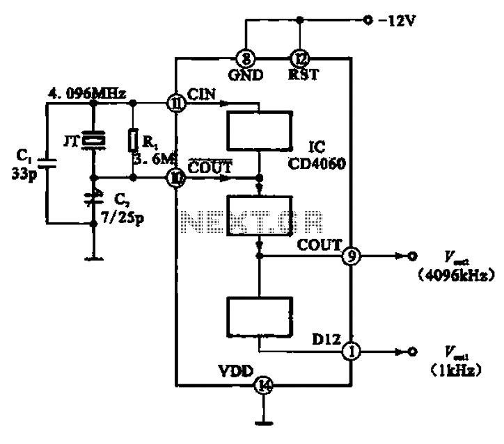
A 1 kHz square wave signal source circuit is illustrated using the CD4060 integrated circuit. The CD4060 operates with an external crystal oscillator and compensating capacitors such as C1 and C2. The internal oscillator circuit of the chip is...
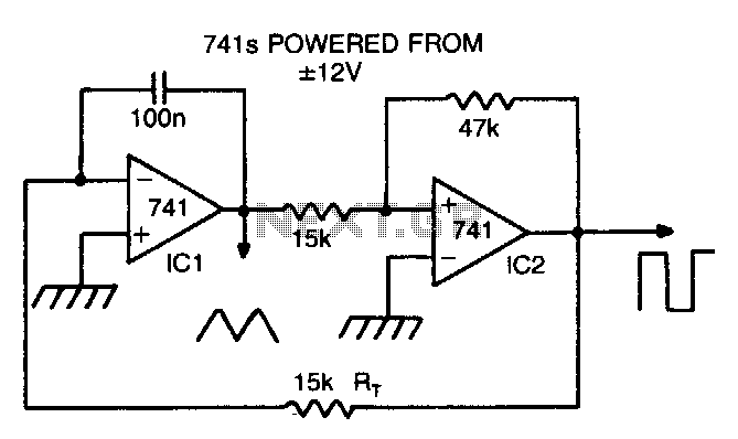
By making Rt variable, it is possible to alter the operating frequency over a 100 to 1 range. The versatile triangle/square wave oscillator has a possible frequency range of 0 Hz to 100 kHz. The described circuit features a variable...
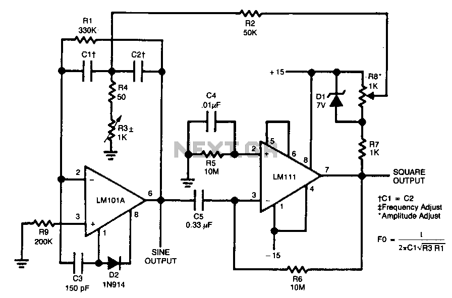
The circuit is designed to generate both sine and square wave outputs for frequencies ranging from below 20 Hz to above 20 kHz. The frequency of oscillation can be easily adjusted by modifying a single resistor, which is a...
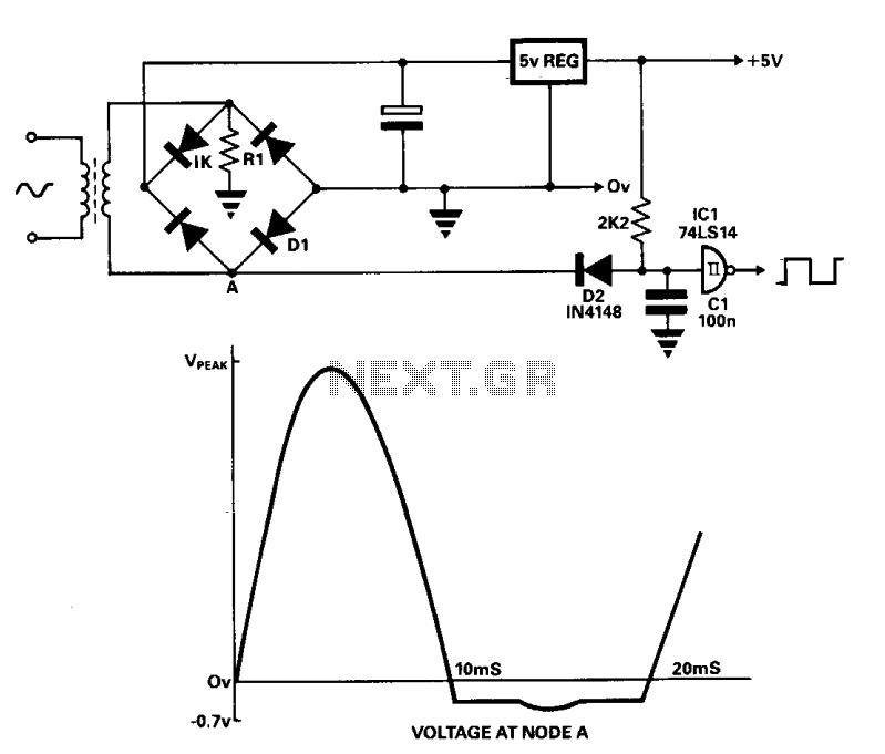
A line frequency square wave with a 1:1 duty cycle can be generated using only three components and a buffer from the power supply. During the alternate half-cycle, point A is clamped to approximately -0.7 V by diode D1...
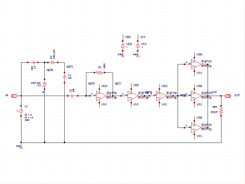
This schematic example demonstrates a sinusoidal voltage input at a frequency of 10 kHz, which is converted to a square wave using an inverter-based circuit. The VDD and VSS rails are connected to +1V and -1V, respectively. The control...
The circuit includes 10K resistors at the bases of the transistors and 1K resistors at the collectors. It is essential to retain these components when relocating the transistors, as omitting the 10K resistors could result in transistor failure, and...