
Sine to Square Wave Converter
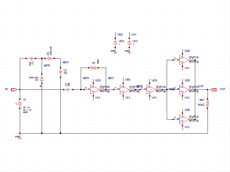
This schematic illustrates a fundamental conversion process where a sinusoidal signal is transformed into a square wave. The circuit employs inverters, which are crucial for this conversion due to their ability to switch the output between high and low states in response to the input signal. The specified frequency of 10 kHz indicates that the input signal oscillates ten thousand times per second, which is a common frequency for digital signal processing applications.
The power supply rails, VDD and VSS, are set to +1V and -1V, respectively, providing the necessary voltage levels for the operation of the inverters. The choice of these voltage levels is essential for ensuring that the inverters operate within their specified parameters, allowing for reliable switching and signal integrity.
The control file referenced contains the model statements for the diodes and MOSFETs integrated into the inverter circuit. These models are crucial for accurately simulating the behavior of the components under various conditions, ensuring that the circuit performs as intended during the simulation phase.
In the simulation mode, voltage markers have been strategically placed at the input (IN) and output (OUT) nodes of the schematic. These markers facilitate real-time monitoring of the voltage levels, allowing for an analysis of how the sinusoidal input is transformed into a square wave output. This setup is vital for validating the performance of the circuit and for troubleshooting any issues that may arise during the simulation process.
Overall, this schematic serves as an effective demonstration of signal conversion techniques, showcasing the interplay between analog and digital signals, and the importance of accurate modeling in circuit design and simulation.This schematic example (see sine2square. png ) demonstrates a sinusoidal voltage input at a frequency of 10KHz converted to a square wave through an inverter-based circuit. VDD and VSS rails are ties to +1V and =1V, respectively. The control file ( sine2square. ctr ) contains model statements for the diodes and the MOS devices used by the inverters. By clicking on the Simulation tab in the Library pane, Gateway switches from capture mode to Simulation Mode ( simulation_mode. png ). The voltage markers have been placed on the input node (IN) and the output node (OUT) on the schematic.
🔗 External reference
Related Circuits
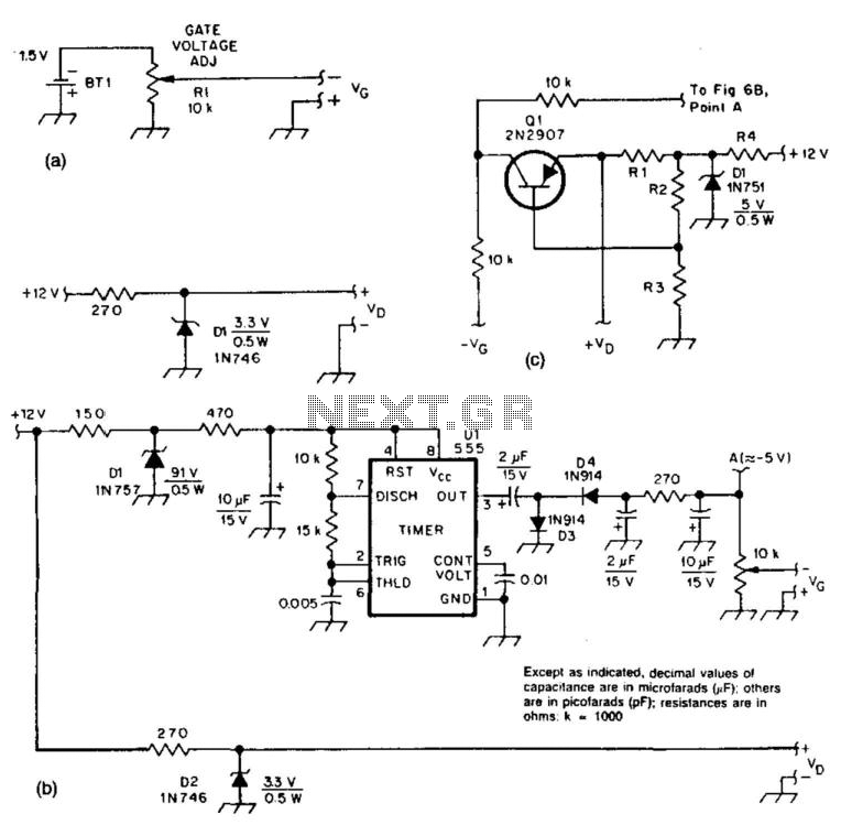
These two circuits provide bias for the microwave preamplifiers discussed in this text. The circuit in Figure 51-5(a) is a simple passive power supply. Figures 51-5(b) and 51-5(c) represent active power supplies, with Ul generating a negative supply and...
This Antenna is most widely used all over the world. For example, when you see a police car it has a transmitter with Ground Pole Antenna. The body of the car serves as ground. It accepts load from a...
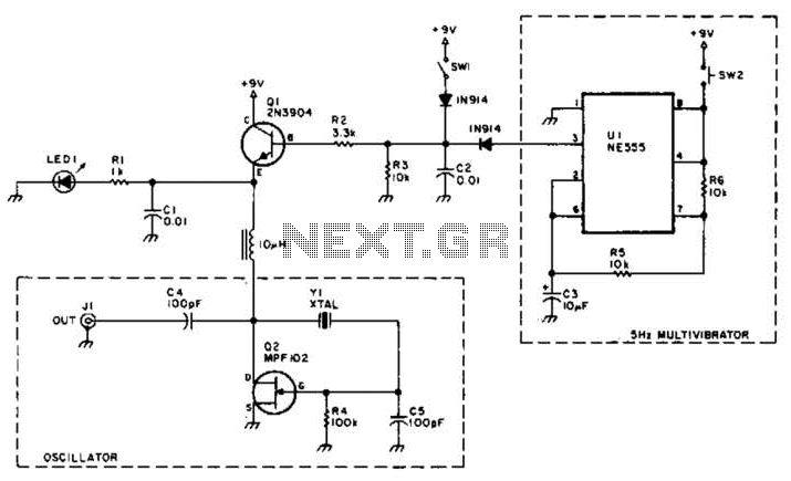
A useful marker oscillator can be constructed using an NE555 timer to generate pulses at an audio frequency. This design facilitates the detection of the signal even amidst interference. The crystal frequency can range from 1 to 30 MHz. The...
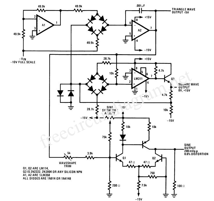
The voltage-to-frequency converter (VFC) in this circuit produces a satisfactory sine-shaped output; however, it lacks good voltage-to-frequency linearity and exhibits a frequency stability of approximately 0.2%. The LM331 is an excellent choice for a linear and stable voltage-to-frequency converter,...
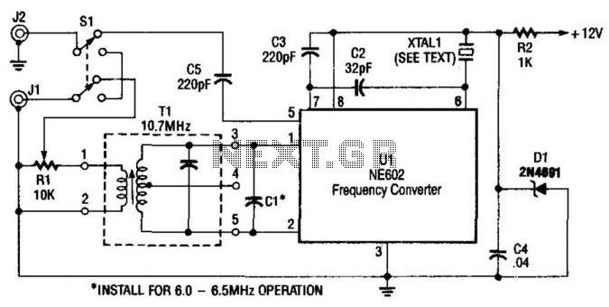
A Signetics NE602 is utilized in this converter to tune the frequency range of 9.5 to 9.8 MHz. An AM car radio functions as a tunable intermediate frequency (IF) amplifier, with the output being taken from J2, the auto...
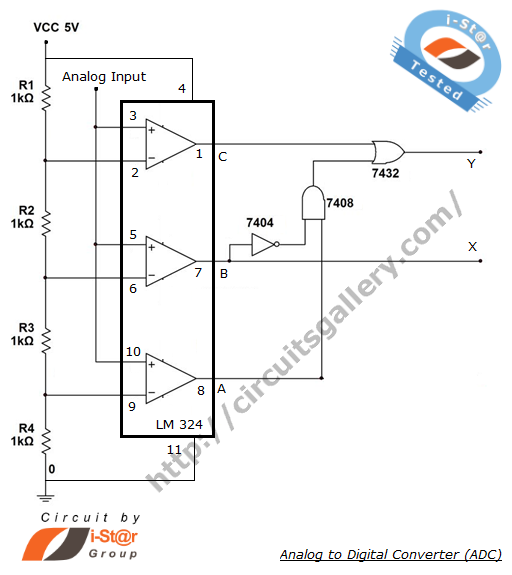
The process of converting an analog voltage into an equivalent digital signal is known as Analog to Digital Conversion (ADC). An ADC is an electronic circuit that converts its analog input to a corresponding binary value. The output depends...
Warning: include(partials/cookie-banner.php): Failed to open stream: Permission denied in /var/www/html/nextgr/view-circuit.php on line 713
Warning: include(): Failed opening 'partials/cookie-banner.php' for inclusion (include_path='.:/usr/share/php') in /var/www/html/nextgr/view-circuit.php on line 713