
Subcarrier Adapter For Fm Tuners Circuit
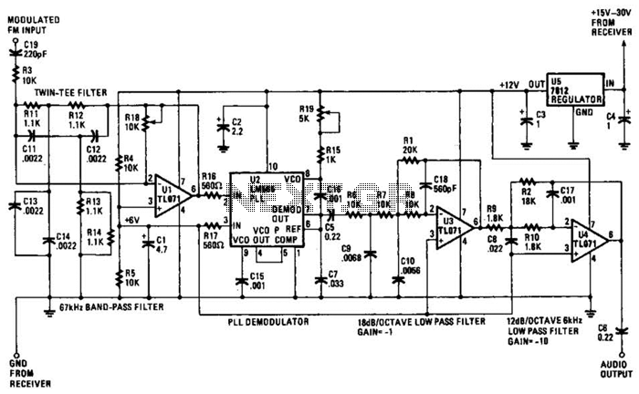
The described circuit utilizes a bandpass filter to isolate a specific frequency range while attenuating unwanted signals. The twin-T network is a classic design for bandpass filtering, utilizing both resistors and capacitors to create a notch filter effect, which is essential for achieving the desired frequency response. The operational amplifier provides necessary gain to ensure that the signal remains strong enough for further processing. The inclusion of the passive filter at the input stage enhances the overall filtering capability, ensuring that low-frequency noise does not interfere with the desired 67 kHz signal.
The LM565 phase-locked loop plays a critical role in demodulating the frequency-modulated signal. By comparing the phase of the incoming signal with that of the VCO, the PLL can lock onto the frequency, allowing for stable demodulation. The adjustable resistor R19 provides flexibility in tuning the VCO frequency, accommodating variations in the incoming signal frequency and ensuring optimal performance of the PLL.
In summary, this circuit effectively combines filtering and modulation techniques to process a 67-kHz frequency-modulated signal, making it suitable for applications requiring precise frequency selection and demodulation. The design highlights the importance of component selection and configuration in achieving desired electronic performance characteristics. Op amp Ul and its associated components comprise the 67-kHz bandpass filter. A twin-T network, comprised of four 1100-12 resistors and four 0.0022- capacitors, is connected in the feedback network of the op amp. That gives some gain at 67 kHz and heavy attenuation for frequencies above and below that frequency. An additional passive filter at the input to the twin-T network (containing a 220-pF capacitor and a 10,000- resistor) provides some additional roll-off for frequencies below 67 kHz.
In practice, the bandpass-filter action covers a frequency range of about 10 kHz above and below the 67-kHz center frequency. Resistor R18 sets the gain of the bandpass-filter stage. Integrated-circuit U2 is a National LM565 phase-locked loop that modulates the 67-kHz fre-quency-modulated (FM) signal from Ul. The LM565 PLL consists of a voltage- controlled oscillator (VCO) set to 67 kHz, and a comparator that compares the incoming frequency-modulated 67-kHz signal at pin 2 with the VCO signal that is fed into pin 5.
The output of the comparator represents the phase difference between the incoming signal and the VCO signal. Therefore, the output is the audio modulated by the subcarrier. A treble deemphasis of 150 is provided by a 0.033- capacitor (at pin 7). The free-miming VCO frequency is determined by the 0.001- capacitor at pin 9 and by the resistance between the positive rail and pin 8 (100 in series with R19).
Variable-resistor R19 adjusts the oscillator frequency (also known as the center frequency`) so that the incoming signal is within the lock range of the PLL. 🔗 External reference
Related Circuits
National Instruments Multisim now features microcontroller unit co-simulation capabilities, enabling the inclusion of a microcontroller, programmed in assembly or C code, within SPICE-modeled circuits. The MCU functionality in Multisim allows students, educators, and professional users to program MCUs in...
Optically isolated phone automatic recording interface circuit, IC3 voice module. The optically isolated phone automatic recording interface circuit is designed to capture audio signals from a telephone line while ensuring electrical isolation between the phone line and the recording device....
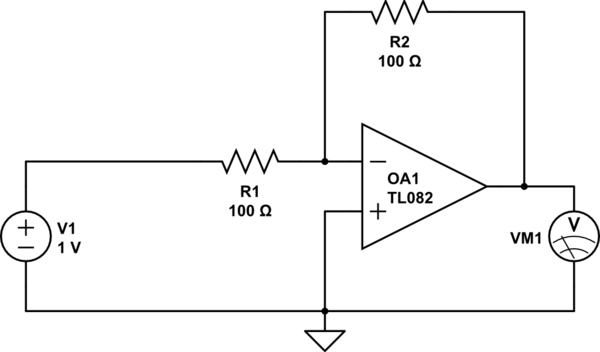
Considering a simple circuit as illustrated below, when the voltage source activates suddenly (changing from 0V to 1V), current will flow through the resistor R1. Assuming an ideal operational amplifier (op-amp) that draws no current, and an ideal voltmeter...

The circuit connection is illustrated in figures a and b. In figure a, a star-shaped winding is used with shunt capacitance, while figure b depicts a triangular winding with capacitance connected in parallel. The working capacitance (Cc) is calculated...
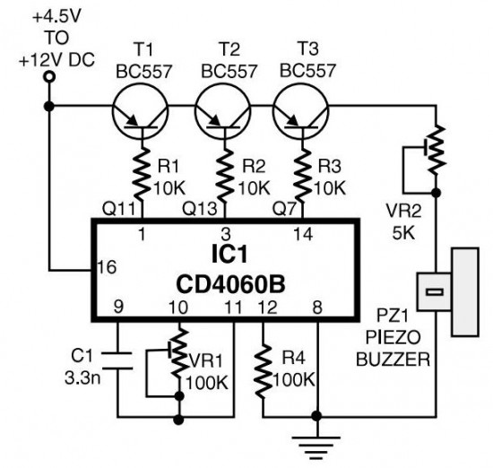
The circuit generates pulses of 1.25 Hz from pin 1 and 20 Hz from pin 14. The three output pins of IC1 are connected to the base terminals of transistors T1, T2, and T3 through resistors R1, R2, and...
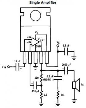
This is a simple mini audio amplifier circuit built around a single LM383 integrated circuit, along with several discrete components to support its operation. The circuit is capable of delivering approximately 7W of audio output. It can be constructed...