
switch debounce circuit
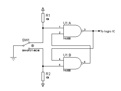
The phenomenon of switch bounce occurs when a mechanical switch is actuated, causing it to make and break contact several times before settling into a stable state. This results in multiple transitions in a very short time, which can be interpreted by digital circuits as multiple signals rather than a single intended action. In applications such as counters, this can lead to erroneous counts, as the counter may increment or decrement multiple times due to the unintended pulses.
To mitigate the effects of switch bounce, a debouncing circuit is commonly employed. The RS latch configuration using NAND gates is one effective method for achieving this. In this setup, the two 2-input NAND gates are connected in such a way that they create a feedback loop. When the switch is pressed, one of the NAND gates changes its output state, which in turn affects the input of the other NAND gate. This feedback mechanism ensures that the output stabilizes quickly, effectively filtering out the rapid fluctuations caused by switch bounce.
The RS latch operates as follows: when the switch is pressed, the first NAND gate detects the change and outputs a low signal. The output of this gate is fed back to the second NAND gate, which alters its output state based on the feedback. This process continues until the switch is released, at which point the circuit returns to its stable state. The result is a clean, debounced signal that can be reliably used in digital applications without the interference of switch bounce.
This debouncing technique is crucial in ensuring the accuracy and reliability of digital systems that rely on mechanical switches, enhancing the overall performance of the electronic circuit.In most digital electronics projects that uses different kinds of switches, switch bounces are commonly encountered. These are extra glitches after the real switch operation. These are tiny pulses that affect the actual operation of the circuit like counters. It is clearly seen that in certain push on the switch, the counting is not accurate. This is causee by the switch bounce. Here now is the image that shows switch bounces and a clean pulse. As you can see in the top image, this is an image of a clean pulse without a switch bounce. On the other hand, below it, shows the bounces formed from switching. The circuit below is a RS latch that is used as a switch debouncer. It`s composed by two 2-input NAND gates with outputs feedbacks to the input of another. (other explation from malvino) 🔗 External reference
Related Circuits
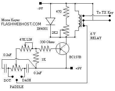
This is not a sophisticated automatic keyer but it is lot QRP to build and to have fun operating it. When the paddle is connected to the DOT terminal, C1 starts to charge. When C1's charge reaches sufficiently high value,...
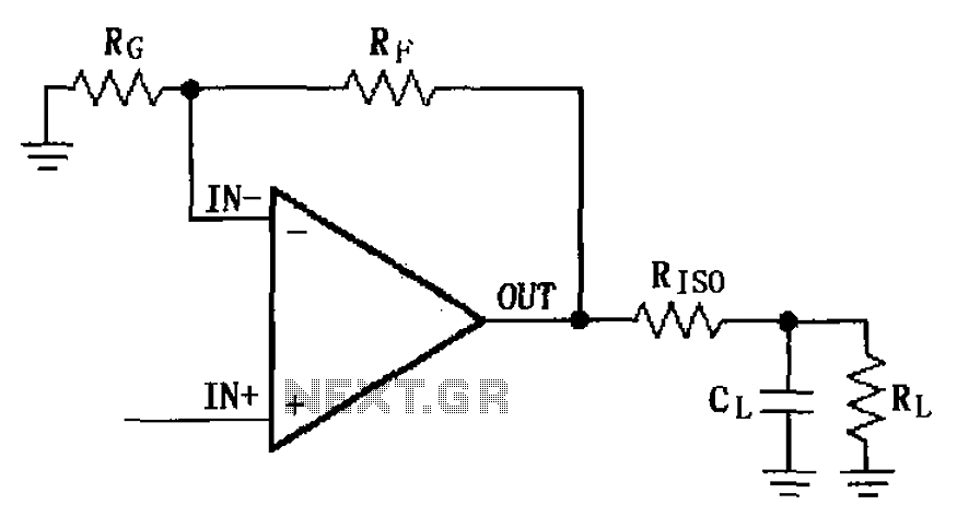
The MAX4223 to MAX4228 series incorporates a capacitive load drive circuit with an isolation resistor (RISO). The maximum allowable capacitive load for these devices is 25pF. However, exceeding this limit can lead to overshoot and ringing. The circuit design...
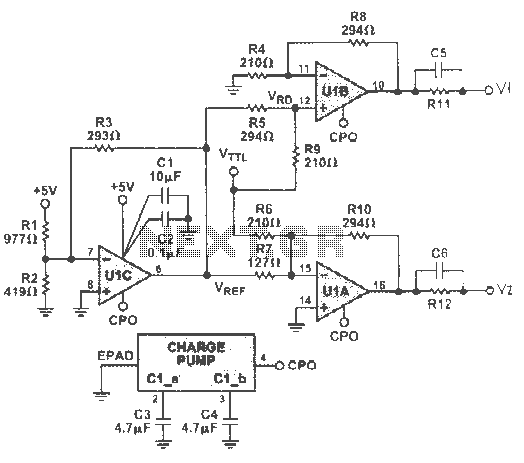
The circuit can incorporate a buffer gate at the input to ensure compatibility with TTL or other logic levels. This design is intended for a TTL 0V circuit to accommodate a 3.5V input signal swing. Additionally, it generates a...

The circuit consists of a radio remote lighting switch utilizing RCM1 type radio-controlled remote control transmitter and receiver components. It features the RCM1A/B component, which facilitates the remote control functionality. Additionally, the design incorporates a remote control transmitter and...
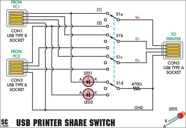
This device enables two computers to share a single USB printer or other USB devices, including external flash drives, memory card readers, or scanners. A rotary switch is used to select the PC that will access the USB device, while...
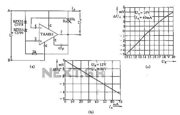
The regulator circuit adjusts the output voltage based on the potentiometer Rp and exhibits linear regulation characteristics. The output voltage Ua varies with the load current Ia, ranging from 0 to 70 mA, as illustrated in Figure (C) for...